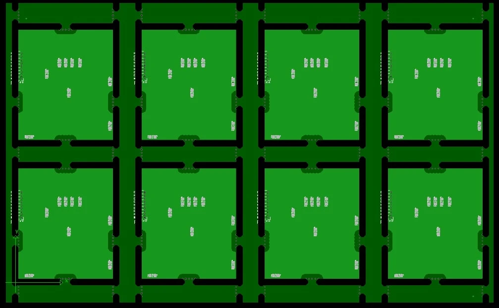
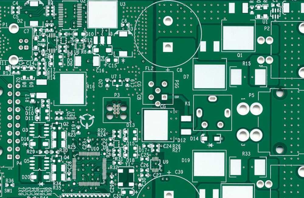
When it comes to PCB manufacturing, designing for panelization is a critical step that can save time, reduce costs, and improve efficiency. But what exactly does this process involve, and how do you ensure your PCB panel size meets the necessary requirements? In this comprehensive guide, we’ll explore PCB design for panelization, including PCB panel size design rules, clearance requirements for PCB panels, PCB panel border dimensions, and design guidelines for PCB panel size. Whether you’re a beginner or a seasoned engineer, this blog will provide actionable insights to optimize your designs for manufacturing success.
What Is PCB Panelization and Why Does It Matter?
PCB panelization is the process of arranging multiple individual printed circuit boards (PCBs) onto a larger panel for manufacturing. This technique allows manufacturers to handle several boards at once, streamlining the fabrication and assembly process. By grouping smaller boards into a single panel, you can reduce material waste, lower production costs, and speed up throughput during automated assembly.
However, panelization isn’t just about placing boards together. It requires careful planning to ensure that the panel size, spacing, and borders meet the manufacturer’s specifications. Poorly designed panels can lead to issues like board damage during depanelization, misalignment during assembly, or even increased production costs due to inefficient layouts. That’s why understanding PCB design for panelization is so important.

Key Benefits of Proper PCB Panelization
Before diving into the technical details, let’s look at why proper panelization is worth the effort:
- Cost Efficiency: Manufacturing multiple boards on a single panel reduces material waste and lowers per-unit costs.
- Faster Production: Panels allow for batch processing, speeding up fabrication and assembly.
- Improved Handling: Larger panels are easier to handle in automated equipment compared to individual small boards.
- Consistency: Uniform panel designs ensure consistent quality across all boards during production.
With these benefits in mind, let’s explore the specific considerations for designing a panel, starting with size rules and guidelines.
PCB Panel Size Design Rules: Getting the Dimensions Right
One of the first steps in PCB design for panelization is determining the appropriate panel size. The size of the panel directly impacts manufacturing efficiency and cost. Here are some key PCB panel size design rules to follow:
1. Understand Standard Panel Sizes
Most PCB manufacturers work with standard panel sizes to maximize their equipment capabilities. Common panel dimensions include 18 x 24 inches (457 x 610 mm) and 21 x 24 inches (533 x 610 mm). However, the usable area within these panels is often smaller due to border and tooling requirements. Typically, the usable area might be reduced by 1-2 inches on each side, leaving an effective working area of around 16 x 22 inches (406 x 559 mm) for a standard 18 x 24-inch panel.
Always check with your manufacturer for their specific panel size constraints before finalizing your design. Using a non-standard size may lead to higher costs or delays.
2. Account for Board Size and Quantity
The size and number of individual PCBs you plan to fit on a panel will dictate the overall panel dimensions. For instance, if your board measures 2 x 3 inches (50 x 75 mm), you can calculate how many boards fit into the usable area of the panel while leaving space for borders and breakaway rails. A good rule of thumb is to maximize the number of boards without overcrowding, as this can lead to issues during depanelization.

3. Consider Panel Strength and Rigidity
Larger panels can sometimes warp or flex during manufacturing, especially if they’re too thin or lack proper support. Ensure your panel thickness (typically between 1.6 mm and 2.0 mm for standard boards) and material (like FR-4) provide enough rigidity. For very large panels, consider adding internal support structures or breakaway rails to maintain stability.
Clearance Requirements for PCB Panels: Avoiding Manufacturing Issues
Another critical aspect of panelization is maintaining proper spacing between individual boards and other elements on the panel. Clearance requirements for PCB panels ensure that boards can be separated without damage and that manufacturing equipment can operate without interference.
1. Spacing Between Individual Boards
The space between individual PCBs on a panel, often called the “breakaway gap,” should typically be at least 0.1 inches (2.5 mm). This clearance allows for clean separation during depanelization, whether using V-scoring or tab routing methods. If the spacing is too tight, there’s a risk of damaging components near the edges during separation.
2. Component Clearance from Board Edges
Components placed too close to the edge of a board can be damaged during depanelization or handling. As a general rule, maintain a clearance of at least 0.2 inches (5 mm) between components and the board edge. For panels using V-scoring, increase this clearance to 0.3 inches (7.5 mm) to account for potential stress during separation.
3. Tooling Holes and Fiducial Marks
Tooling holes and fiducial marks are essential for aligning the panel during manufacturing and assembly. Ensure there’s at least 0.15 inches (3.8 mm) of clearance around tooling holes to avoid interference with other elements. Fiducial marks should also have a clear zone of at least 0.1 inches (2.5 mm) around them for accurate machine vision recognition.

PCB Panel Border Dimensions: Defining the Edges
The borders of a PCB panel, also known as process edges or rails, play a vital role in handling and stability during manufacturing. Properly defined PCB panel border dimensions ensure the panel can be processed without issues.
1. Minimum Border Width
Borders typically need to be at least 0.5 inches (12.7 mm) wide on all sides of the panel. This space accommodates tooling holes, fiducial marks, and test points, and provides a gripping area for automated equipment. Narrower borders may lead to handling difficulties or insufficient space for manufacturing aids.
2. Breakaway Rails for Small Boards
For panels with very small individual boards, additional breakaway rails (also called mouse bites) may be added along the borders. These rails are usually 0.2 to 0.3 inches (5 to 7.5 mm) wide and include perforated tabs for easy removal after assembly. They help maintain panel integrity during processing.
3. Avoiding Overly Large Borders
While wider borders can improve handling, they also reduce the usable area for PCBs, potentially increasing costs. Strike a balance by adhering to the manufacturer’s minimum border requirements while maximizing the number of boards per panel.
Design Guidelines for PCB Panel Size: Best Practices
Beyond specific measurements, there are several design guidelines for PCB panel size that can help you create efficient and manufacturable panels. These best practices are based on common industry standards and aim to minimize errors during production.
1. Optimize for Depanelization Methods
The method used to separate individual boards from the panel—such as V-scoring or tab routing—affects panel design. For V-scoring, ensure boards are aligned in straight rows and columns with consistent spacing. For tab routing, leave space for router paths (typically 0.1 inches or 2.5 mm wide) between boards. Consult your manufacturer to choose the best method for your design.
2. Balance Panel Utilization
Aim to use as much of the usable panel area as possible without violating clearance or border rules. For example, if your board is 2 x 2 inches (50 x 50 mm), arrange them in a grid to fit the maximum number within the usable area, leaving at least 0.1 inches (2.5 mm) between boards for separation.
3. Consider Assembly Requirements
If your panel will go through automated assembly, ensure the design accommodates pick-and-place machines and reflow soldering processes. This includes placing fiducial marks in visible locations (usually near the panel corners) and ensuring components are not too close to breakaway edges, as mentioned earlier.

Common Mistakes to Avoid in PCB Panelization
Even with the best intentions, mistakes in panel design can lead to costly delays or defective boards. Here are some pitfalls to watch out for:
- Ignoring Manufacturer Guidelines: Every manufacturer has specific panelization requirements. Failing to follow them can result in rejected designs or additional fees.
- Insufficient Clearance: Placing boards or components too close together increases the risk of damage during separation or assembly.
- Overloading the Panel: Trying to fit too many boards on a panel can compromise structural integrity and make handling difficult.
- Forgetting Tooling Features: Omitting tooling holes or fiducial marks can cause alignment issues during production.
Tools and Software for PCB Panelization Design
Designing a panel manually can be time-consuming and error-prone. Thankfully, most PCB design software includes features or plugins for panelization. These tools allow you to arrange boards, define borders, add breakaway rails, and check clearances automatically. When using such tools, input the manufacturer’s panel size and spacing requirements to ensure compatibility.
Additionally, many manufacturers offer panelization services or templates. Submitting your individual board design and letting them handle the panel layout can save time, especially for complex or high-volume projects.
Final Thoughts on Designing for Panelization
Designing for panelization is a crucial step in PCB manufacturing that directly impacts cost, efficiency, and quality. By following PCB panel size design rules, adhering to clearance requirements for PCB panels, and defining proper PCB panel border dimensions, you can create panels that streamline production and minimize errors. Remember to consult your manufacturer early in the design process to align with their capabilities and avoid surprises.
Whether you’re working on a small prototype or a large-scale production run, applying these design guidelines for PCB panel size will help you achieve better results. With careful planning and attention to detail, your PCB design for panelization can lead to smoother manufacturing and a more reliable end product.
 ALLPCB


