 ALLPCB


In the world of printed circuit board (PCB) design, layer thickness plays a critical role in determining signal integrity and overall performance. Whether you're working on high-speed PCB design or a simple prototype, understanding how PCB layer thickness affects signal integrity, impedance, and signal loss is essential. Factors like dielectric thickness, copper thickness, and PCB stackup design directly influence how well your board performs, especially in demanding applications. In this comprehensive guide, we’ll break down these elements and explain their impact with practical insights and data to help you optimize your designs for success.
Why PCB Layer Thickness Matters for Signal Integrity
PCB layer thickness isn’t just a physical characteristic; it’s a key factor that influences electrical performance. Signal integrity refers to the quality of an electrical signal as it travels through the board. Poor signal integrity can lead to data errors, noise, and system failures, especially in high-speed designs. The thickness of various layers, including the dielectric material and copper traces, directly affects how signals propagate and interact with each other.
For instance, in high-speed PCB design, signals can travel at speeds close to the speed of light, and even small variations in layer thickness can cause delays or distortions. A well-designed PCB stackup with balanced layer thicknesses ensures minimal signal loss and maintains impedance control, which is vital for reliable performance. Let’s dive deeper into the specific aspects of layer thickness and their effects.
Understanding PCB Stackup Design and Layer Thickness
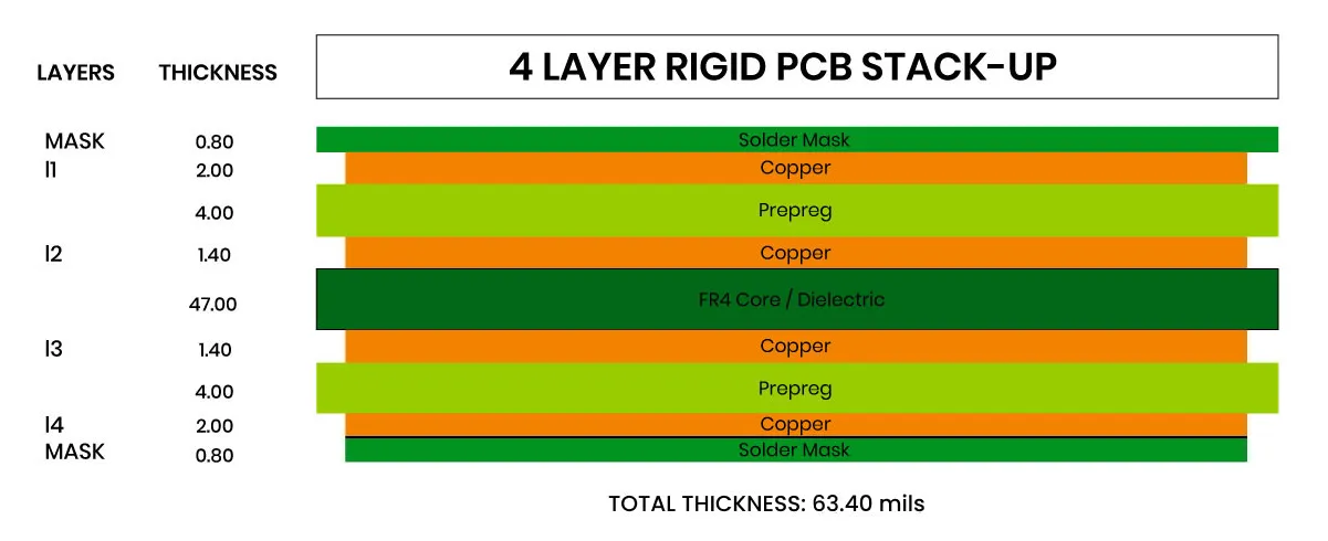
PCB stackup design refers to the arrangement of copper and dielectric layers in a board. A typical stackup might include multiple layers of conductive copper separated by insulating dielectric materials. The thickness of each layer in this stackup impacts signal transmission, power distribution, and electromagnetic interference (EMI) control.
For a standard 4-layer PCB, a common stackup might look like this:
- Top Layer (Signal): 1 oz copper (approximately 35 micrometers thick)
- Dielectric Layer 1: 0.2 mm thick
- Inner Layer 1 (Ground): 1 oz copper
- Dielectric Layer 2: 0.8 mm thick
- Inner Layer 2 (Power): 1 oz copper
- Dielectric Layer 3: 0.2 mm thick
- Bottom Layer (Signal): 1 oz copper
In this setup, the dielectric thickness between layers determines the capacitance and impedance of the traces, while copper thickness affects current-carrying capacity and signal loss. A balanced stackup ensures that signals travel with minimal interference, especially in high-speed applications where timing is critical.
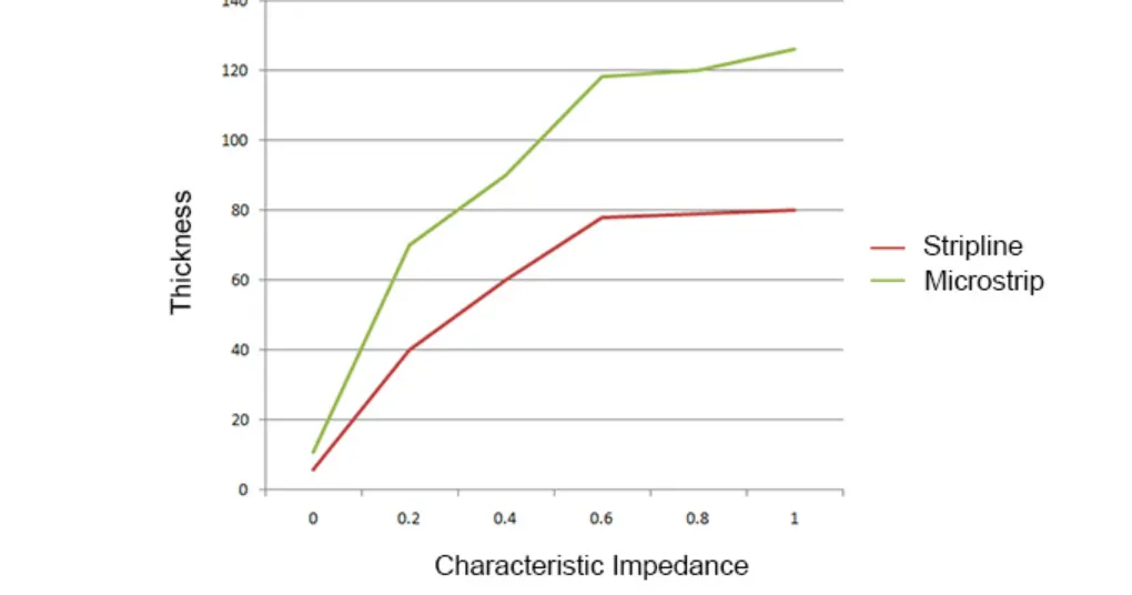
Dielectric Thickness and Impedance Control
Dielectric thickness, the insulating material between copper layers, is a major factor in controlling impedance. Impedance is the resistance to the flow of alternating current in a circuit, and maintaining a consistent impedance (often 50 ohms for high-speed signals) is crucial for signal integrity. If the dielectric thickness varies, it can lead to impedance mismatches, causing signal reflections and data errors.
The relationship between dielectric thickness and impedance can be understood through a simple formula for a microstrip trace:
Z = 87 / sqrt(Er + 1.41) * ln(5.98 * H / (0.8 * W + T))
Where:
- Z = Impedance (ohms)
- Er = Dielectric constant of the material (e.g., 4.2 for FR-4)
- H = Dielectric thickness (mils or mm)
- W = Trace width (mils or mm)
- T = Copper thickness (mils or mm)
From this formula, it’s clear that increasing dielectric thickness (H) raises impedance, while a thinner dielectric lowers it. For high-speed PCB design, a dielectric thickness of 4-6 mils (0.1-0.15 mm) is often used between signal and ground planes to achieve a 50-ohm impedance with standard trace widths. If the dielectric is too thick, signals may experience higher impedance, leading to mismatches. Conversely, if it’s too thin, crosstalk between layers can increase.
Choosing the right dielectric material and thickness is critical. Materials like FR-4 are common for their cost-effectiveness, but for high-frequency designs, low-loss materials with stable dielectric constants are preferred to minimize signal distortion.
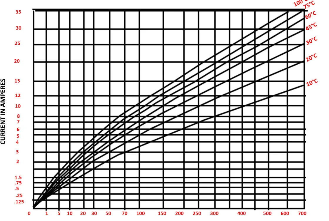
Copper Thickness and Signal Loss
Copper thickness, measured in ounces per square foot (oz/ft2), determines how much current a trace can carry and how much signal loss occurs due to resistance. Common copper thicknesses are 1 oz (35 micrometers), 2 oz (70 micrometers), and 0.5 oz (17.5 micrometers). While thicker copper is great for high-current applications, it can introduce challenges for high-speed signals.
Signal loss in copper traces is primarily due to the skin effect at high frequencies. The skin effect causes current to flow near the surface of the conductor, increasing effective resistance. For a 1 oz copper trace at 1 GHz, signal loss might be around 0.2 dB per inch, but this can double with thinner copper or higher frequencies. Thicker copper reduces resistive losses, but it can also affect impedance calculations and make fine trace geometries harder to achieve.
In high-speed PCB design, balancing copper thickness with trace width and dielectric spacing is key. For instance, a 1 oz copper layer paired with a 5-mil wide trace on a 4-mil thick dielectric often works well for 50-ohm impedance in high-speed applications. However, increasing copper thickness to 2 oz may require wider traces or adjusted dielectric spacing to maintain the same impedance, which can complicate the design.
Impact of Layer Thickness on High-Speed PCB Design
High-speed PCB design, often involving signals above 100 MHz, demands precise control over layer thickness to prevent issues like crosstalk, reflections, and timing skew. In such designs, signal integrity is highly sensitive to variations in dielectric and copper thickness. Even a 10% variation in dielectric thickness can cause a noticeable shift in impedance, leading to signal reflections that degrade performance.
For example, in a high-speed design for a 5 Gbps data rate, the signal wavelength is short, and any mismatch in layer thickness can cause significant delays. A common practice is to use thinner dielectric layers (around 3-5 mils) between signal and ground planes to tightly couple the signal to its return path, reducing EMI and crosstalk. Additionally, maintaining symmetry in the PCB stackup design ensures that signals on different layers experience similar propagation delays, which is critical for differential pairs.
Another consideration is the impact of layer thickness on thermal management. Thicker dielectric layers can trap heat, while thinner layers improve heat dissipation but may compromise mechanical strength. Balancing these factors is essential for reliable high-speed designs.
Practical Tips for Optimizing PCB Layer Thickness
Designing a PCB with optimal layer thickness requires careful planning and attention to detail. Here are some actionable tips to help you achieve better signal integrity and performance:
- Define Impedance Requirements Early: Use simulation tools to calculate the required dielectric thickness and trace width for your target impedance (e.g., 50 ohms). Stick to these values during layout.
- Choose the Right Dielectric Material: For high-speed designs, consider low-loss materials with a stable dielectric constant to minimize signal distortion.
- Balance Copper Thickness: Use 1 oz copper for most signal layers, but opt for 2 oz or higher for power traces to handle larger currents without excessive heat.
- Maintain Stackup Symmetry: Ensure that dielectric thicknesses are consistent across layers to avoid signal skew and mechanical stress during manufacturing.
- Collaborate with Manufacturers: Work closely with your PCB fabrication team to confirm achievable layer thicknesses and material options before finalizing your design.
By following these guidelines, you can create a PCB stackup design that supports both signal integrity and mechanical reliability, even in complex high-speed applications.
Common Challenges and Solutions in Layer Thickness Design
Designing for optimal PCB layer thickness isn’t without challenges. One common issue is manufacturing variability. Even if you specify a dielectric thickness of 5 mils, actual boards may vary by ±10%, affecting impedance. To mitigate this, design with tolerances in mind and use controlled impedance traces where precision is critical.
Another challenge is cost. Thinner dielectric layers and specialized materials often increase production costs. For budget-conscious projects, consider hybrid stackups where only critical layers use high-performance materials, while others rely on standard options like FR-4.
Finally, thermal expansion can cause issues in multi-layer boards with uneven layer thicknesses. Different materials expand at different rates, leading to warping. Using symmetrical stackups and selecting materials with compatible thermal properties can help avoid this problem.
Conclusion: Mastering PCB Layer Thickness for Optimal Performance
PCB layer thickness is a fundamental aspect of design that directly impacts signal integrity and performance. From dielectric thickness influencing impedance to copper thickness affecting signal loss, every detail matters, especially in high-speed PCB design. By understanding the principles of PCB stackup design and applying practical strategies, you can create boards that deliver reliable performance in any application.
Whether you’re tackling a simple 2-layer board or a complex 12-layer design, paying attention to layer thickness ensures minimal signal distortion, reduced EMI, and improved overall functionality. With the insights and tips provided in this guide, you’re well-equipped to optimize your next PCB project for success. Focus on precision, collaborate with your manufacturing team, and leverage simulation tools to fine-tune your designs for the best possible outcomes.


