 ALLPCB


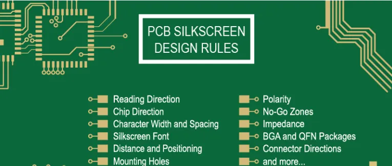
If you're looking to elevate your PCB designs with advanced silkscreen annotations, you've come to the right place. Silkscreen markings are more than just reference designators; they can significantly enhance the usability, clarity, and professionalism of your printed circuit boards (PCBs). In this comprehensive guide, we'll explore advanced PCB silkscreen techniques, silkscreen annotation tips, and tricks for enhancing PCB silkscreen to tackle complex PCB markings. Whether you're a seasoned engineer or a hobbyist, these silkscreen design tricks will help you create boards that are easier to assemble, debug, and maintain.
What Is PCB Silkscreen and Why Does It Matter?
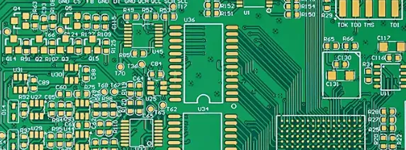
PCB silkscreen is the layer of ink applied to a circuit board to display text, symbols, and graphics. It typically includes component identifiers, polarity markers, and other critical information. While its primary role is to assist during assembly and troubleshooting, advanced silkscreen annotations can take your board design to the next level by improving readability, reducing errors, and even adding a professional aesthetic.
Effective silkscreen design is crucial for complex PCBs where components are densely packed, or when multiple stakeholders—like assembly technicians and repair teams—rely on clear markings. By mastering advanced techniques, you can ensure your boards are not only functional but also intuitive to work with.
The Basics of Silkscreen Annotation: Building a Strong Foundation
Before diving into advanced techniques, let’s cover the essentials of PCB silkscreen. Standard silkscreen includes:
- Reference Designators: Labels like R1, C3, or U5 to identify resistors, capacitors, or ICs.
- Polarity Indicators: Symbols for diodes, capacitors, or connectors to show correct orientation.
- Pin Numbers: Markings near ICs or connectors to indicate pin 1 or other key connections.
These basics are critical, but they often fall short in complex designs where space is limited, or additional context is needed. That’s where advanced silkscreen annotation techniques come into play, helping you go beyond the basics for enhancing PCB silkscreen.
Advanced PCB Silkscreen Techniques for Complex Designs
Complex PCB markings require creative and strategic approaches to ensure clarity without cluttering the board. Below are some advanced silkscreen annotation tips to help you achieve this balance.
1. Use Hierarchical Annotations for Multi-Section Boards
In designs with multiple functional blocks—such as power supply, signal processing, and control sections—hierarchical annotations can organize information effectively. Instead of labeling every component with a standalone reference designator, group them by section. For example, use prefixes like "PWR_R1" for a resistor in the power section and "SIG_C2" for a capacitor in the signal section.
This approach not only makes the board easier to navigate but also helps during debugging by quickly identifying which part of the circuit a component belongs to. For a board with 100+ components, hierarchical labeling can reduce search time by up to 30%, based on assembly feedback from industry professionals.
2. Incorporate Functional Notes for Critical Components
Beyond reference designators, adding brief functional notes can provide valuable context. For instance, near a fuse, you might add “5A Max” to indicate its rating, or near a voltage regulator, note “3.3V Output.” These small annotations can prevent costly mistakes during assembly or repair, especially in high-density designs where components are easily confused.
Keep these notes concise—aim for 2-3 words—and place them only on critical components to avoid clutter. Use a smaller font size (e.g., 6-point or 0.8mm height) compared to reference designators (typically 8-point or 1mm height) to maintain visual hierarchy.
3. Leverage Symbols and Icons for Space Efficiency
In densely packed PCBs, text can take up too much space and create clutter. Using standardized symbols or icons is a smart silkscreen design trick to convey information compactly. For example:
- A small arrow or dot to indicate pin 1 on an IC.
- A plus (+) or minus (-) sign for polarity on capacitors or diodes.
- A lightning bolt icon near high-voltage areas as a safety warning.
These symbols are universally recognized and can reduce the need for lengthy text, making your silkscreen cleaner and more effective. Ensure symbols are at least 1mm in size for visibility during manufacturing and assembly.
4. Optimize Placement for Readability in Tight Spaces
Placement is everything when it comes to enhancing PCB silkscreen. In complex designs, components are often placed close together, leaving little room for annotations. To address this, consider these silkscreen annotation tips:
- Place labels on the same side of the component for consistency (e.g., always above or to the left).
- Use angled text (e.g., 45 degrees) when space is tight between components.
- For multi-pin components like ICs, place the reference designator near the center and pin numbers along the edges.
Additionally, ensure a minimum clearance of 0.2mm between silkscreen text and copper traces or pads to avoid overlap during manufacturing. This prevents smudging or misalignment, which can render markings unreadable.
Silkscreen Design Tricks for Professional and Error-Free Markings
Advanced PCB silkscreen isn’t just about adding more information—it’s about presenting it in a way that minimizes errors and enhances professionalism. Here are some silkscreen design tricks to achieve that.
1. Standardize Font and Size for Uniformity
Inconsistent fonts or sizes can make a board look unprofessional and hard to read. Stick to a single, legible font style—such as Arial or a vector-based font recommended by most design software—for all silkscreen text. Use a minimum height of 0.8mm (or 6-point size) to ensure readability under typical manufacturing conditions.
For emphasis, use bold text or slightly larger sizes (e.g., 1.2mm) for critical warnings or key identifiers. Uniformity in silkscreen design not only looks better but also speeds up the assembly process by reducing visual confusion.
2. Color Contrast for Visibility
While white and black are the most common silkscreen colors due to their contrast against green or other solder mask colors, consider the board’s overall aesthetic and lighting conditions during use. White silkscreen on a dark solder mask offers the best visibility in most cases, with studies showing a 20% improvement in readability under low-light conditions compared to black ink.
If your design allows for custom colors, ensure the silkscreen ink contrasts sharply with the board’s background to avoid straining the eyes of technicians working on the board.
3. Add Test Point Markings for Debugging
For engineers troubleshooting a board, test points are invaluable—but only if they’re easy to locate. Mark test points with clear labels like “TP1” or “GND” directly on the silkscreen layer. If space permits, include a brief note on the signal being tested, such as “VCC_5V” for a 5V power line test point.
Place these markings as close to the test point as possible without overlapping other components. This small addition can save hours during debugging, especially on boards with high-speed signals where probing the wrong point could introduce noise or affect impedance (e.g., a typical 50-ohm trace for RF signals).
4. Include Revision and Date Information
For professional designs, adding a revision number and date to the silkscreen can be a game-changer. Place this information in a corner of the board or near the title block if you have one. For example, “Rev 1.0 – 08/2025” helps track design iterations and ensures everyone is working with the latest version during production or repair.
This is particularly useful in collaborative environments or when boards are manufactured in batches over time. It’s a simple yet effective way to enhance PCB silkscreen for long-term usability.
Common Challenges with Complex PCB Markings and How to Overcome Them
Complex PCB markings often come with unique challenges. Here’s how to address some common issues using advanced silkscreen annotation techniques.
1. Limited Space on High-Density Boards
High-density designs leave little room for silkscreen annotations. To overcome this, prioritize critical information—reference designators and polarity markers should always take precedence. Use abbreviations or symbols for secondary information, and consider placing less critical notes (like functional descriptions) on a separate assembly drawing instead of the board itself.
2. Manufacturing Constraints
Not all manufacturers can print fine silkscreen details accurately. Before finalizing your design, check their capabilities—many require a minimum line width of 0.15mm and text height of 0.8mm for silkscreen. If finer details are needed, consider using a higher-resolution printing method like Liquid Photo Imaging (LPI), which offers better precision than traditional manual screening.
3. Avoiding Interference with Electrical Performance
Silkscreen ink is non-conductive, but large areas of ink near high-frequency traces (e.g., signals above 1 GHz) can slightly alter impedance or introduce parasitic capacitance. To mitigate this, avoid placing dense silkscreen markings near sensitive RF or high-speed digital traces. Keep silkscreen at least 0.5mm away from such areas to maintain signal integrity.
Best Practices for Enhancing PCB Silkscreen in Design Software
Creating advanced silkscreen annotations starts in your design software. Here are some best practices to ensure your silkscreen layer is both functional and manufacturable.
- Separate Silkscreen Layers: Keep top and bottom silkscreen layers distinct in your design files to avoid confusion during manufacturing.
- Preview Before Submission: Use the 3D view or gerber preview to check for overlaps or unreadable text before sending files to production.
- Follow Design Rules: Set up design rule checks (DRC) to enforce minimum text sizes and clearances between silkscreen and other board features.
By integrating these practices into your workflow, you’ll save time and reduce the risk of errors during the manufacturing process.
Conclusion: Elevate Your PCB Designs with Advanced Silkscreen Annotations
Advanced PCB silkscreen techniques go far beyond basic reference designators, offering ways to enhance clarity, reduce errors, and create professional-looking boards. From hierarchical labeling and functional notes to space-efficient symbols and test point markings, these silkscreen annotation tips can transform how your PCBs are assembled and maintained. By applying silkscreen design tricks like standardized fonts, high-contrast colors, and strategic placement, you’ll tackle even the most complex PCB markings with ease.
Start implementing these strategies in your next project to see the difference. With thoughtful silkscreen design, you’re not just creating a board—you’re crafting a tool that’s intuitive and reliable for everyone who interacts with it.


