ALLPCB


Switch-mode power supplies (SMPS) are the backbone of modern electronics, providing efficient power conversion for countless devices. However, ensuring power integrity in these systems is crucial to minimize issues like power loss, electromagnetic interference (EMI), and unstable operation. In this comprehensive guide, we’ll explore actionable techniques to improve power integrity in SMPS designs, focusing on key aspects such as power electronic PCB layout, pulse width modulation (PWM) optimization, and EMI reduction. Whether you’re an engineer or a designer, this article will help you build more reliable and efficient power systems.
What Is Power Integrity in Switch-Mode Power Supplies?
Power integrity refers to the quality and stability of power delivery in an electronic system. In switch-mode power supplies, maintaining power integrity means ensuring that the output voltage remains stable despite rapid switching, load changes, and external noise. Poor power integrity can lead to voltage ripples, power loss, and even system failures. By focusing on design elements like PCB layout and component selection, you can significantly enhance the performance of your SMPS.
Why Power Integrity Matters for SMPS
Switch-mode power supplies operate by rapidly switching between on and off states to regulate voltage, which introduces challenges like high-frequency noise and EMI. These issues can interfere with other components in a circuit, degrade efficiency through power loss, and cause unreliable operation. Improving power integrity not only ensures stable power delivery but also extends the lifespan of your system and reduces the risk of costly redesigns.
In the sections below, we’ll break down practical strategies to tackle these challenges, with a focus on long-tail keywords like switch-mode power supply design, power loss reduction, EMI mitigation, power electronic PCB layout techniques, and PWM optimization.
Key Challenges in Switch-Mode Power Supply Design
Before diving into solutions, it’s important to understand the main challenges that affect power integrity in SMPS:
- Power Loss: Inefficient switching and parasitic effects in components lead to energy dissipation as heat, reducing overall efficiency.
- Electromagnetic Interference (EMI): High-frequency switching generates noise that can interfere with nearby circuits or violate regulatory standards.
- Voltage Ripples: Rapid switching can cause fluctuations in output voltage, affecting the performance of downstream components.
- Thermal Stress: Excessive power loss and poor layout can create hot spots, stressing components and reducing reliability.
Addressing these challenges requires a combination of careful design practices and strategic component placement, which we’ll explore next.
Techniques to Improve Power Integrity in SMPS
1. Optimize Power Electronic PCB Layout
The layout of your printed circuit board (PCB) plays a critical role in maintaining power integrity in a switch-mode power supply. A poorly designed layout can amplify EMI, increase power loss, and introduce noise into the system. Here are some proven power electronic PCB layout tips:
- Minimize Loop Areas: The high-frequency switching currents in an SMPS flow through loops formed by the switching transistor, diode, and output capacitor. Keep these loops as small as possible to reduce inductance and EMI. For example, place the input capacitor close to the switching transistor to shorten the current path.
- Use Ground Planes: A solid ground plane helps provide a low-impedance return path for currents, reducing noise and improving power integrity. Avoid splitting the ground plane under high-current paths, as this can disrupt return currents and increase EMI.
- Separate High and Low Current Paths: Route high-current switching paths away from sensitive analog or control circuitry to prevent noise coupling. For instance, keep the feedback loop traces short and away from the inductor.
- Place Decoupling Capacitors Strategically: Position decoupling capacitors near the power pins of integrated circuits to filter out high-frequency noise. Use a combination of ceramic capacitors with low equivalent series resistance (ESR) for effective noise suppression.
By focusing on these layout practices, you can significantly reduce parasitic inductance and capacitance, which are common causes of power loss and EMI in SMPS designs.
2. Reduce Power Loss with Component Selection
Power loss in a switch-mode power supply often stems from inefficiencies in components like transistors, diodes, and inductors. Selecting the right parts can make a big difference in overall performance. Consider these tips:
- Choose Low RDS(on) MOSFETs: For switching transistors, select MOSFETs with low on-resistance (RDS(on)) to minimize conduction losses. For example, a MOSFET with an RDS(on) of 10 mΩ can reduce power dissipation compared to one with 50 mΩ under the same load conditions.
- Use Low-ESR Capacitors: Output capacitors with low equivalent series resistance (ESR) reduce ripple voltage and power loss. Ceramic or tantalum capacitors are often good choices for SMPS applications.
- Select High-Efficiency Inductors: Inductors with low DC resistance (DCR) and high saturation current ratings help minimize losses in the magnetic core and windings. Look for inductors designed for high-frequency operation to match the switching frequency of your SMPS.
By prioritizing efficiency in component selection, you can cut down on heat generation and improve the overall power integrity of your design.
3. Mitigate EMI in Switch-Mode Power Supplies
Electromagnetic interference is a major concern in SMPS due to the rapid switching of currents, which generates high-frequency noise. Reducing EMI not only improves power integrity but also ensures compliance with regulatory standards. Here are some effective strategies:
- Add Snubber Circuits: A snubber circuit, typically consisting of a resistor and capacitor, can dampen voltage spikes caused by switching transients. For example, a snubber with a 10 nF capacitor and a 100 Ω resistor can reduce ringing at the switching node.
- Use Shielding and Filtering: Incorporate EMI filters at the input and output stages of your SMPS to block high-frequency noise. Additionally, consider using ferrite beads in series with input lines to suppress conducted EMI.
- Optimize Switching Frequency: Adjusting the switching frequency can help avoid interference with sensitive frequency bands in your system. For instance, increasing the frequency to 500 kHz or higher can push EMI harmonics out of the audible range or critical communication bands.
- Route Traces Carefully: Avoid running high-frequency signal traces over splits in the ground plane, as this can create radiating loops that amplify EMI. Keep traces short and direct to minimize their antenna-like behavior.
Implementing these EMI reduction techniques ensures cleaner power delivery and prevents interference with other parts of your system.
4. Fine-Tune Pulse Width Modulation (PWM) Control
Pulse width modulation (PWM) is the heart of most switch-mode power supplies, controlling the duty cycle to regulate output voltage. Optimizing PWM settings can enhance power integrity by reducing ripple and improving transient response. Consider these approaches:
- Adjust Duty Cycle for Efficiency: A well-tuned duty cycle minimizes switching losses while maintaining stable output. For example, operating at a 50% duty cycle in a buck converter can balance conduction and switching losses for optimal efficiency.
- Use Soft Switching Techniques: Implement zero-voltage switching (ZVS) or zero-current switching (ZCS) to reduce switching losses and EMI. These techniques ensure that the transistor switches when voltage or current is near zero, cutting down on energy dissipation.
- Stabilize Feedback Loops: Design the feedback loop to respond quickly to load changes without introducing oscillations. Use appropriate compensation components (e.g., resistors and capacitors in the feedback network) to achieve a phase margin of at least 45 degrees for stability.
By refining PWM control, you can achieve tighter voltage regulation and better power integrity in your SMPS.
5. Manage Thermal Performance
Heat is a byproduct of power loss in switch-mode power supplies, and excessive temperatures can degrade components and reduce reliability. Effective thermal management is essential for maintaining power integrity. Try these methods:
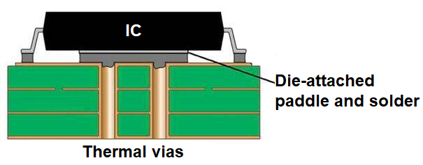
- Use Thermal Vias: Place thermal vias under high-power components like MOSFETs to transfer heat to the opposite side of the PCB or to a heat sink. For example, a grid of 0.3 mm vias with 1.2 mm spacing can improve heat dissipation.
- Incorporate Heat Sinks: Attach heat sinks to components that generate significant heat, ensuring proper airflow around the SMPS to prevent thermal buildup.
- Optimize Component Placement: Avoid clustering heat-generating components together. Spread them out on the PCB to distribute heat evenly and prevent hot spots.
Good thermal design keeps your SMPS operating within safe temperature limits, preserving power integrity over the long term.
Tools and Simulations for Power Integrity Analysis
Designing for power integrity in switch-mode power supplies often requires simulation tools to predict and analyze performance before prototyping. These tools can help identify potential issues with EMI, power loss, and voltage stability early in the design process.
- SPICE Simulations: Use SPICE-based simulators to model the transient behavior of your SMPS, including voltage ripples and switching losses. You can simulate different load conditions to ensure stable operation.
- EMI Analysis Tools: Specialized software can predict radiated and conducted EMI based on your PCB layout and component choices, allowing you to make adjustments before testing.
- Thermal Modeling Software: Tools for thermal analysis can map out heat distribution on your PCB, helping you optimize component placement and heat dissipation strategies.
Investing time in simulations can save significant resources by reducing the need for multiple hardware iterations.
Common Mistakes to Avoid in SMPS Design
Even experienced engineers can overlook critical details that impact power integrity. Here are some common pitfalls to steer clear of:
- Ignoring Parasitic Effects: Parasitic inductance and capacitance in traces and components can cause voltage spikes and ringing. Always account for these effects during layout and component selection.
- Overloading Components: Choosing components with insufficient current or voltage ratings can lead to failures under load. Always select parts with a safety margin, such as a capacitor rated for 25V in a 12V system.
- Neglecting Feedback Loop Design: A poorly designed feedback loop can cause instability, leading to output voltage oscillations. Test and tune the loop for optimal response.
By avoiding these mistakes, you can build a more robust and efficient switch-mode power supply.
Conclusion: Building Reliable Switch-Mode Power Supplies
Improving power integrity in switch-mode power supplies is a multifaceted task that requires attention to PCB layout, component selection, EMI mitigation, PWM optimization, and thermal management. By implementing the techniques outlined in this guide, such as minimizing loop areas in power electronic PCB layouts, selecting low-loss components, and fine-tuning PWM control, you can reduce power loss, suppress EMI, and ensure stable power delivery.
At ALLPCB, we understand the importance of precision in power supply design. Whether you’re working on a small prototype or a large-scale production run, focusing on power integrity from the start will save time, reduce costs, and result in a more reliable product. Start applying these strategies in your next project to achieve better performance and efficiency in your SMPS designs.