ALLPCB


Flexible printed circuit boards (PCBs) are revolutionizing modern electronics, enabling compact, lightweight, and dynamic designs in devices like wearables, smartphones, and medical implants. However, their unique properties—thin, bendable substrates like polyimide or polyester—make them prone to damage during assembly if not handled with care. For engineers, assembling flexible PCBs without compromising their integrity is critical to ensuring performance and reliability. In this guide, we'll walk you through the essential steps, best practices, and common pitfalls to avoid when assembling flexible PCBs, drawing from industry standards and practical insights.
Our goal is to equip you with actionable techniques to protect these delicate circuits during assembly, backed by specific examples and data. Whether you're working on a prototype or scaling up production, these strategies will help you achieve high-quality results.
Why Flexible PCBs Require Special Handling
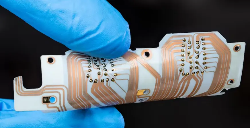
Flexible PCBs differ significantly from rigid PCBs due to their material composition and physical properties. Typically made from polyimide films with thicknesses ranging from 0.05 mm to 0.2 mm, they can bend, fold, and conform to complex shapes. However, this flexibility comes with vulnerabilities:
- Material Sensitivity: Polyimide is susceptible to tearing, cracking, or delamination under excessive mechanical stress.
- Thermal Sensitivity: Flexible substrates can deform or degrade at high temperatures, with some materials withstanding only up to 260°C during soldering.
- Component Placement Challenges: Bending zones must remain free of components to prevent solder joint failures, requiring precise placement.
Improper handling during assembly can lead to defects like cracked traces, lifted pads, or compromised electrical connectivity. For example, exceeding the minimum bend radius—often calculated as 10 times the board thickness for dynamic applications—can cause copper traces to fracture, leading to open circuits. Understanding these risks is the first step to successful assembly.
Step-by-Step Guide to Assembling Flexible PCBs
To assemble flexible PCBs without damage, follow these carefully designed steps. Each phase requires attention to detail and specialized techniques to protect the board's integrity.
1. Design Verification and Preparation
Before assembly begins, verify that the PCB design is optimized for manufacturability and flexibility. Key considerations include:
- Bend Radius Compliance: Ensure the design adheres to the minimum bend radius. For a 0.1 mm thick single-layer flex PCB, the static bend radius should be at least 1 mm, while dynamic applications may require 2 mm or more.
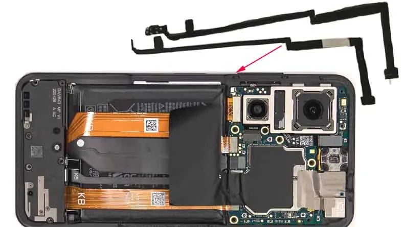
- Component Placement: Place components in static areas, avoiding bending zones. Use stiffeners (e.g., FR-4 or polyimide) in regions with connectors or fine-pitch components to reduce strain.
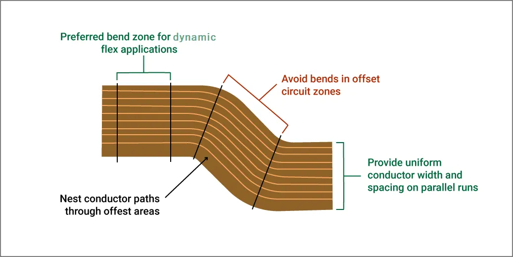
- Trace Routing: Use curved traces instead of sharp angles to minimize stress concentration. Stagger traces in multilayer designs to prevent "I-beaming," where stacked copper layers increase rigidity.
Example: In a wearable fitness tracker, designers placed the microcontroller on a stiffened section of the PCB, while the flexible portion routed signals to sensors, maintaining a bend radius of 1.5 mm to ensure durability during wrist movement.
Review the design using CAD tools like KiCAD or Altium Designer, and perform a Design for Manufacturing (DFM) check to confirm compliance with assembly house rules, such as minimum via distances (typically 0.3 mm from bend areas).
2. Material Handling and Storage
Flexible PCBs are delicate and require careful handling to prevent physical damage. Follow these best practices:
- Use Cleanroom Protocols: Handle boards in a cleanroom (Class 1000 or better) to avoid contamination. Wear ESD-safe gloves to prevent static discharge, which can damage sensitive components.
- Store Properly: Store flex PCBs flat in antistatic bags or trays at a temperature of 15–25°C and humidity below 60%. Flexibility comes with vulnerabilities. Avoid stacking heavy items on top, as this can cause creasing.
- Minimize Bending Before Assembly: Keep boards flat during transport and inspection. Repeated flexing before soldering can weaken the substrate.
Example: A manufacturer reported a 15% reduction in assembly defects after implementing flat storage trays and limiting pre-assembly handling to trained personnel.
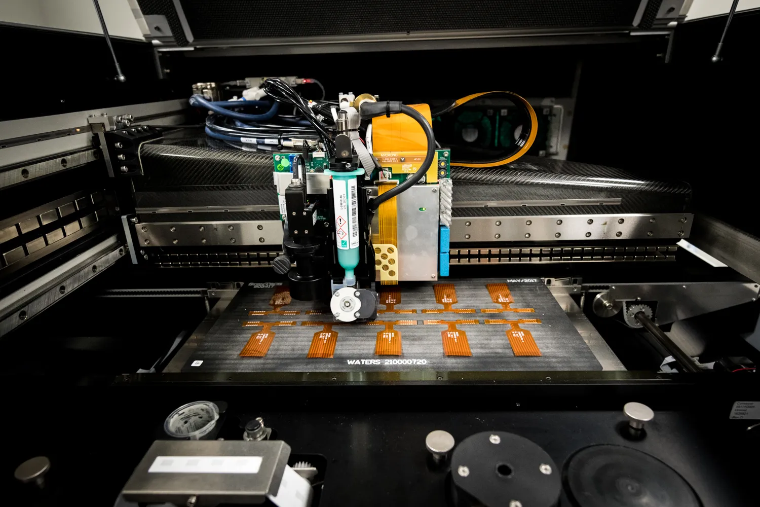
3. Component Placement with Precision
Accurate component placement is critical to avoid stress on the flexible substrate. Use automated pick-and-place machines equipped with vision systems to ensure precision:
- Low-Pressure Placement: Set pick-and-place machines to apply minimal force (e.g., 1–2 N) to avoid denting the substrate.
- Stiffener Support: Apply temporary or permanent stiffeners before placement in areas with fine-pitch components, such as 0.5 mm BGA packages, to prevent flexing during soldering.
- Alignment Checks: Use fiducial markers (0.5–1 mm in diameter) to align components accurately, reducing placement errors to within 50 µm.
Example: In a medical sensor assembly, engineers used a polyimide stiffener under a 0.4 mm pitch sensor chip, achieving a placement accuracy of 25 µm and eliminating solder joint failures.
4. Soldering with Controlled Thermal Profiles
Soldering is one of the most critical stages, as excessive heat can damage the flexible substrate or components. Use these techniques:
- Reflow Soldering for SMT: Employ a reflow oven with a precise thermal profile. For lead-free soldering, maintain a peak temperature of 245–260°C for no more than 10 seconds to avoid substrate warping. Use a slow ramp-up rate (1–2°C/s) to minimize thermal shock.
- Low-Temperature Solder: For heat-sensitive substrates, consider low-temperature solder alloys like Sn42Bi58, which melt at 138°C, reducing the risk of damage.
- Custom Fixtures: Use jigs or clamping mechanisms to hold the PCB flat during soldering without applying excessive pressure. Ensure fixtures are heat-resistant to withstand дальше reflow temperatures.
Example: A study showed that using a 10-zone reflow oven with a tailored profile reduced solder joint defects by 20% in flex PCB assemblies compared to a standard 6-zone oven.
5. Inspection and Testing
Post-assembly inspection ensures the PCB is free of defects and performs as intended. Implement these quality control measures:
- Automated Optical Inspection (AOI): Use AOI systems to detect misaligned components, solder bridges, or lifted pads. Set resolution to 10 µm for fine-pitch components.
- Bend Testing: Perform static or dynamic bend tests to verify the PCB's flexibility. For dynamic applications, test up to 10,000 cycles at the specified bend radius (e.g., 2 mm) to ensure no trace cracking.
- Electrical Continuity Testing: Use flying probe testers to check for open or short circuits, ensuring 100% connectivity across traces with resistances as low as 0.1 Ω.
Example: A smartphone manufacturer identified 5% of flex PCBs with micro-cracks using X-ray inspection, allowing rework before integration, saving $10,000 in potential recalls.
Common Pitfalls to Avoid
Even with careful planning, mistakes during flex PCB assembly can lead to costly failures. Here are the top pitfalls and how to avoid them:
- Overbending During Handling: Avoid flexing the PCB beyond its designed bend radius during assembly. Train personnel to handle boards flat and use fixtures to maintain shape.
- Inadequate Stiffener Use: Failing to apply stiffeners in high-stress areas can cause component detachment. Always use stiffeners for connectors or ICs with pitches below 0.8 mm.
- Improper Thermal Profiles: Overheating during reflow can degrade polyimide substrates. Always validate thermal profiles using thermocouples placed on the PCB (target accuracy: ±2°C).
- Ignoring Design Rules: Violating DFM rules, such as placing vias in bending zones, can lead to cracking. Ensure vias are at least 0.3 mm from flex areas, per IPC-6013 standards.
Example: A wearable device prototype failed after 500 bend cycles due to vias placed 0.1 mm from a bending zone, highlighting the importance of adhering to IPC standards.
How ALLPCB Supports Flexible PCB Assembly
For engineers seeking reliable flex PCB assembly, partnering with a trusted manufacturer is key. ALLPCB offers advanced manufacturing capabilities tailored to flexible PCBs, including quick-turn prototyping, high-precision component placement, and global logistics. Our state-of-the-art facilities ensure compliance with IPC-6013 standards, while our DFM analysis helps identify potential issues before production, reducing defects by up to 30%. Whether you're developing a compact medical device or a foldable consumer gadget, ALLPCB's expertise streamlines the process, delivering high-quality assemblies on time.
Conclusion
Assembling flexible PCBs without damage requires a combination of careful design, precise handling, and controlled processes. By verifying designs, using proper materials, employing specialized equipment, and conducting rigorous testing, engineers can achieve reliable, high-performance assemblies. Avoiding common pitfalls like overbending or improper soldering further ensures success. With these strategies, you're well-equipped to tackle the challenges of flex PCB assembly and bring innovative designs to life.
For your next project, consider leveraging professional manufacturing services to optimize quality and efficiency. Have questions or tips to share? Let us know in the comments below!