ALLPCB


Are you struggling with component placement accuracy in PCB assembly? Automated lines are the game-changer you’ve been looking for. They tackle key challenges like precision, calibration, and tolerance with cutting-edge technology, ensuring faster production and fewer errors. In this blog, we dive deep into how automated systems, including pick and place machines, solve these issues for electrical engineers. We’ll explore practical solutions, technical insights, and actionable tips to optimize your PCB assembly process.
Why Component Placement Challenges Matter in PCB Assembly
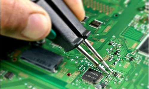
For electrical engineers, the precision of component placement in printed circuit board (PCB) assembly is critical. A single misaligned component can lead to signal interference, short circuits, or complete board failure. With modern electronics shrinking in size—think smartphones with components as small as 0.4mm x 0.2mm—manual placement is no longer viable. Automated lines address these challenges head-on, offering speed and automated component placement accuracy that manual processes can’t match.
In this post, we’ll break down the specific hurdles in component placement and how automation conquers them. From machine calibration to surface-mount technology (SMT) tolerances, we’ve got you covered with detailed insights tailored for engineers.
Key Challenges in Component Placement for PCB Assembly
Before diving into solutions, let’s identify the core challenges electrical engineers face during PCB assembly:
- Precision Issues: Misplacement by even 0.1mm can disrupt connections, especially for fine-pitch components like QFNs or BGAs.
- Speed vs. Accuracy: High-speed production often sacrifices precision, leading to defects in mass production.
- Component Variety: PCBs often include a mix of SMT and through-hole components, each requiring different handling.
- Machine Calibration: Poorly calibrated machines result in consistent placement errors, costing time and resources.
- Tolerance Limits: Tight SMT component placement tolerance levels are hard to maintain without advanced systems.
These challenges can delay projects, increase costs, and frustrate engineers. Thankfully, automated assembly lines, especially those with advanced pick and place machines, provide reliable solutions.
How Automated Lines Solve Component Placement Challenges
Automated PCB assembly lines use sophisticated technology to address the issues mentioned above. Let’s explore how they boost efficiency and accuracy with a focus on key areas like pick and place machine precision and calibration.
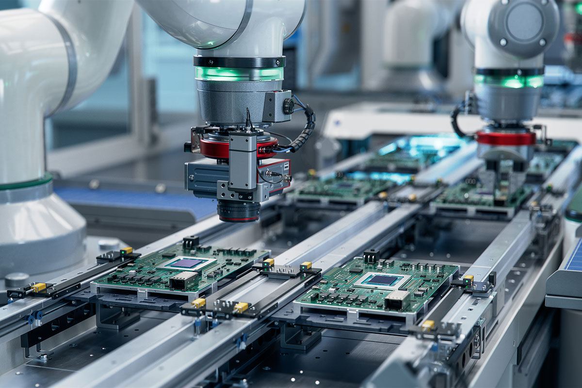
1. Achieving Unmatched Automated Component Placement Accuracy
Modern pick and place machines are designed to place components with pinpoint accuracy, often within ±0.01mm. They use vision systems—cameras and sensors—to detect board fiducials (reference points) and align components accordingly. For instance, a high-end machine can place up to 200,000 components per hour while maintaining this precision, a feat impossible by hand.
For engineers, this means fewer defects and less rework. Imagine assembling a board for a medical device where a misplaced capacitor could cause failure. Automated systems ensure that every component, from a 0402 resistor to a complex IC, lands exactly where it should.
Practical Tip: When selecting a pick and place machine, check for vision system capabilities. Machines with dual-camera setups (one for the board, one for the component) offer better automated component placement accuracy.
2. Mastering Automated Component Placement Machine Calibration
Calibration is the backbone of any automated system. If a machine is off by even a fraction of a millimeter, every placement will be incorrect. Automated lines often include self-calibration features, using test boards to adjust for any drift in alignment over time. For example, some machines run a calibration cycle every 10,000 placements to maintain consistency.
As an engineer, you’ve likely encountered calibration issues during long production runs. A poorly calibrated machine might place a 0.5mm pitch component slightly off, leading to soldering defects during reflow. Automated systems minimize this risk by continuously monitoring and adjusting their settings.
Actionable Advice: Schedule regular maintenance for your automated equipment. Use calibration jigs—special boards with known reference points—to verify automated component placement machine calibration weekly. This small step can save hours of troubleshooting later.
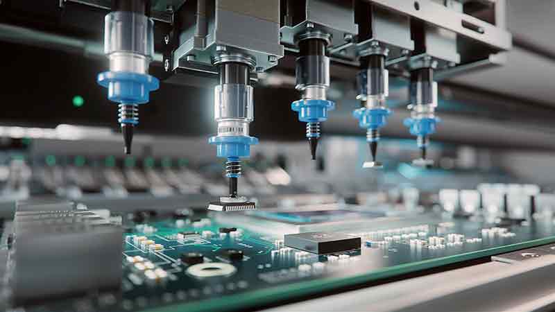
3. Meeting Tight SMT Component Placement Tolerance
Surface-mount technology (SMT) components often have extremely tight tolerances. A typical SMT design might require a placement tolerance of ±0.05mm to ensure proper soldering and functionality. Automated lines excel here by using precision nozzles and programmable settings to handle components of varying sizes and shapes.
For instance, when assembling a PCB for automotive electronics, you might deal with components that must withstand vibrations and temperature swings. If placement exceeds the SMT component placement tolerance, the solder joint could fail under stress. Automated systems reduce this risk by consistently meeting or exceeding tolerance specs.
Engineer’s Note: Always review your PCB design files (like Gerber files) to confirm that fiducial marks are clear and correctly positioned. This helps the machine maintain tight tolerances during placement.
4. Enhancing Pick and Place Machine Precision
The heart of any automated line is the pick and place machine. Precision in these machines comes from a combination of mechanical design, software algorithms, and feedback systems. High-end models use linear motors instead of traditional belts, reducing vibration and improving pick and place machine precision to within ±0.005mm in some cases.
Consider a real-world scenario: assembling a high-density PCB for a 5G device. These boards often have hundreds of components packed into a small area, with spacing as tight as 0.3mm. A precise pick and place machine ensures that each part is positioned correctly, avoiding overlap or misalignment that could disrupt high-frequency signals.
Pro Tip: Invest in machines with real-time error detection. If a component is picked incorrectly or dropped, the system can halt and alert you, preventing further errors.
Benefits of Automated Lines for Electrical Engineers
Switching to or optimizing automated PCB assembly lines offers several advantages for engineers working on complex projects:
- Time Savings: Automated systems can reduce assembly time by up to 80% compared to manual methods, allowing you to meet tight deadlines.
- Cost Efficiency: Fewer defects mean less rework and waste. For a batch of 10,000 boards, even a 1% defect rate reduction can save thousands of dollars.
- Scalability: Automated lines handle both small prototypes and large-scale production runs without sacrificing quality.
- Data Insights: Many systems log placement data, helping you identify patterns in errors or inefficiencies for continuous improvement.
For example, an engineer I worked with on a consumer electronics project reported a 30% drop in production time after upgrading to a machine with enhanced vision systems. The data logs also helped us tweak the PCB layout to reduce placement errors by another 15%.
Common Pitfalls and How to Avoid Them
Even with automation, things can go wrong. Here are some pitfalls to watch for and how to address them:
- Incorrect Feeder Setup: If feeders (which hold components for the machine) are loaded wrong, placement errors occur. Double-check part numbers and orientations before starting a run.
- Poor Board Design: Missing fiducials or unclear markings can confuse the vision system. Ensure your design follows best practices for automation.
- Neglecting Maintenance: Dust or wear on machine parts can degrade precision. Follow the manufacturer’s maintenance schedule to keep pick and place machine precision intact.
Future Trends in Automated PCB Assembly
The field of PCB assembly is evolving rapidly, and automation is at the forefront. Here are a few trends electrical engineers should watch:
- AI Integration: Artificial intelligence is being used to predict and correct placement errors before they happen, further improving automated component placement accuracy.
- Smaller Components: As devices shrink, machines are adapting to handle 01005 components (0.4mm x 0.2mm) with even tighter tolerances.
- IoT Connectivity: Machines connected to the Internet of Things (IoT) provide real-time data to engineers, enabling remote monitoring and adjustments.
Staying ahead of these trends can give your projects a competitive edge, especially in industries like IoT or wearable tech where precision is non-negotiable.
Conclusion: Elevate Your PCB Assembly with Automation
Component placement challenges in PCB assembly don’t have to slow you down. Automated lines, with their focus on automated component placement accuracy, automated component placement machine calibration, SMT component placement tolerance, and pick and place machine precision, offer reliable solutions for electrical engineers. By investing in the right equipment, maintaining rigorous calibration schedules, and following design best practices, you can boost efficiency, reduce errors, and deliver high-quality boards every time.
Ready to take your PCB assembly to the next level? Start by evaluating your current setup and exploring automated systems that fit your needs. Have a tip or experience to share about automated assembly? Drop it in the comments—we’d love to hear from you!