In the world of electronics manufacturing, protecting sensitive components from environmental hazards is crucial for ensuring reliability and longevity. One of the most effective methods to achieve this is through the vacuum potting process. But what exactly is vacuum potting, and how does it help in achieving void-free potting for electronics? Simply put, vacuum potting is a technique that uses a vacuum environment to encapsulate electronic components with a protective compound, eliminating air bubbles or voids that could compromise performance. This process offers numerous benefits, including enhanced protection, improved thermal conductivity, and superior structural integrity.
In this comprehensive guide, we’ll break down the vacuum potting process, explore the benefits of vacuum encapsulation, dive into potting compound degassing, and provide actionable tips for troubleshooting potting voids. Whether you're an engineer, a manufacturer, or someone curious about advanced encapsulation techniques, this blog will equip you with the knowledge to achieve superior results in electronic protection.
What Is Vacuum Potting and Why Does It Matter?
Vacuum potting is a specialized encapsulation method used to protect electronic assemblies from moisture, dust, vibrations, and temperature extremes. Unlike standard potting, which is done under normal atmospheric conditions, vacuum potting involves placing the electronic component and potting compound in a vacuum chamber. This removes trapped air from the compound and the assembly, ensuring a void-free finish.
Voids, or air bubbles, in potting material can lead to serious issues. They can reduce thermal conductivity, potentially causing overheating in components that generate heat, such as power transistors or microcontrollers. Voids can also compromise electrical insulation, leading to short circuits or signal degradation. For instance, a void near a high-voltage component could lower the dielectric strength, increasing the risk of arcing. Additionally, voids weaken the structural integrity of the encapsulation, making it prone to cracking under mechanical stress.
By eliminating these air pockets, vacuum potting ensures that the protective layer around electronics is uniform and robust. This is especially critical in industries like automotive, aerospace, and medical devices, where reliability can be a matter of safety.
The Vacuum Potting Process: Step-by-Step
Understanding the vacuum potting process is essential for achieving consistent, high-quality results. Below is a detailed breakdown of the steps involved in this technique, tailored to help you grasp each phase clearly.
1. Preparation of Components and Materials
Before potting begins, the electronic assembly must be thoroughly cleaned to remove dust, grease, or contaminants that could interfere with adhesion. The potting compound, often a two-part resin like epoxy, silicone, or polyurethane, is mixed according to the manufacturer’s specifications. Proper mixing is crucial to ensure uniform curing and to avoid inconsistencies in the final encapsulation.
2. Degassing the Potting Compound
Potting compound degassing is a critical step in achieving void-free potting for electronics. During mixing, air can become entrapped in the liquid resin. To remove these air bubbles, the mixed compound is placed in a vacuum chamber. The reduced pressure causes the trapped air to expand and rise to the surface, where it is released. This step typically takes a few minutes, depending on the compound’s viscosity and the vacuum level, often around 29 inches of mercury (inHg) or roughly 98 kPa of negative pressure.
3. Placement in the Vacuum Chamber
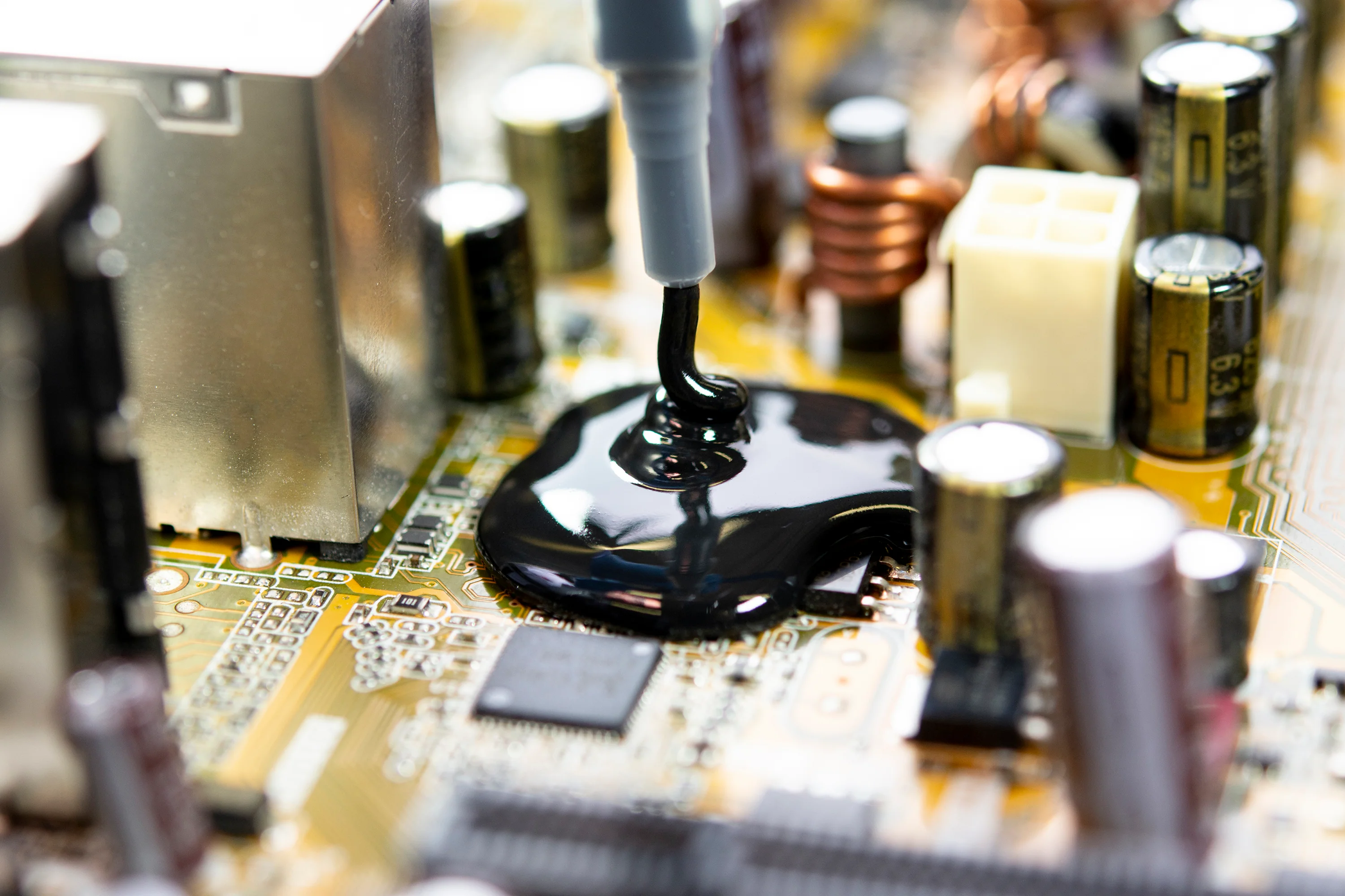
Once degassed, the potting compound is poured over the electronic assembly, which is positioned inside a mold or enclosure. The entire setup is then placed back into the vacuum chamber. The vacuum is applied again to remove any remaining air trapped between the components or within tight spaces, such as under circuit boards or around pins.
4. Curing the Compound
After the vacuum process, the assembly is removed from the chamber and allowed to cure. Curing can occur at room temperature or in an oven, depending on the compound used. For example, some epoxy resins cure in 24 hours at 25°C, while others may require 2 hours at 60°C for faster processing. The vacuum ensures that no air bubbles form during curing, resulting in a solid, uniform encapsulation.
Key Benefits of Vacuum Encapsulation
The vacuum encapsulation benefits are numerous, making it a preferred choice for high-reliability applications. Let’s explore some of the most significant advantages this method offers.
1. Elimination of Voids for Enhanced Protection
As mentioned earlier, voids in potting material can create weak points. Vacuum potting ensures a bubble-free encapsulation, providing a seamless barrier against moisture ingress, which can cause corrosion or electrical shorts. For example, in automotive electronics exposed to humidity levels of 85% or higher, void-free potting can prevent failures that might otherwise occur within months.
2. Improved Thermal Management
Electronic components often generate heat during operation. Voids in potting material act as insulators, trapping heat and potentially causing components to exceed their maximum operating temperature (often around 85°C to 125°C for many ICs). Vacuum potting creates a uniform layer with better thermal conductivity, helping to dissipate heat more effectively. This can extend the lifespan of components by reducing thermal stress.
3. Superior Electrical Insulation
Air pockets in potting material can lower the dielectric strength, increasing the risk of electrical breakdown. Vacuum encapsulation ensures consistent insulation, which is vital for high-voltage applications. For instance, in power electronics handling voltages above 600V, a void-free potting layer can maintain insulation resistance values exceeding 10 MΩ, ensuring safe operation.
4. Enhanced Mechanical Strength
A uniform potting layer provides better resistance to vibrations and mechanical shocks, which are common in industrial or transportation environments. This is especially important for components mounted in vehicles, where vibrations can reach frequencies of 10-55 Hz during operation. Vacuum potting minimizes the risk of cracks or delamination, ensuring long-term durability.
Potting Compound Degassing: Why It’s a Game-Changer
Potting compound degassing is often overlooked, yet it plays a pivotal role in achieving void-free potting for electronics. When mixing resins and hardeners, air inevitably gets trapped in the liquid. If this air isn’t removed before potting, it can form bubbles during curing, leading to the issues we’ve discussed.
Degassing under vacuum reduces the pressure around the compound, allowing air bubbles to expand and escape. The process is particularly effective for high-viscosity compounds, which are more prone to trapping air. For example, a silicone compound with a viscosity of 10,000 cP (centipoise) may require 5-10 minutes of degassing at a vacuum level of 29 inHg to ensure complete air removal.
Proper degassing not only prevents voids but also improves the flow of the compound into tight spaces on the circuit board. This ensures complete coverage, even in complex assemblies with densely packed components or fine-pitch connectors.
Troubleshooting Potting Voids: Common Issues and Solutions
Even with vacuum potting, achieving a perfect result isn’t always guaranteed. Troubleshooting potting voids requires identifying the root cause and applying the right fix. Below are common problems and practical solutions to ensure void-free encapsulation.
1. Incomplete Degassing of the Compound
If the potting compound isn’t fully degassed, air bubbles will remain and form voids during curing. To avoid this, always degas the compound until no more bubbles rise to the surface. Monitor the vacuum level and extend degassing time if needed, especially for thicker materials. A typical benchmark is to degas until the compound appears clear and bubble-free under inspection.
2. Insufficient Vacuum Level
A weak vacuum may not remove all trapped air from the assembly. Ensure your vacuum chamber reaches a pressure low enough to extract air from tight spaces, typically around 29 inHg. Regularly calibrate and maintain the vacuum equipment to avoid leaks or performance issues that could compromise the process.
3. Improper Pouring Technique
Pouring the potting compound too quickly or from a height can introduce new air bubbles. Pour slowly and close to the surface of the assembly to minimize air entrapment. Using a dispensing nozzle or syringe can help control the flow and reduce turbulence.
4. Complex Geometry of Components
Assemblies with intricate designs, such as those with tall components or deep cavities, are prone to trapping air. To address this, consider tilting the mold during pouring to allow air to escape. Additionally, applying vacuum in multiple stages—once before pouring and again after—can help ensure complete air removal.
5. Curing Issues
If the compound cures too quickly, air may not have time to escape under vacuum. Check the curing time and temperature recommendations for your material. Some compounds allow for a slower cure at room temperature to give trapped air more time to release during the vacuum phase.
Best Practices for Void-Free Potting in Electronics
To maximize the effectiveness of vacuum potting, follow these best practices tailored for electronics manufacturing:
- Choose the Right Compound: Select a potting material with appropriate viscosity and curing properties for your application. Low-viscosity compounds flow better into tight spaces, reducing the risk of voids.
- Maintain Equipment: Regularly inspect and maintain your vacuum chamber and dispensing tools to ensure consistent performance.
- Control Environmental Factors: Work in a clean, temperature-controlled environment to avoid contamination or premature curing of the compound.
- Test Small Batches: Before full-scale production, test the potting process on a small batch to identify potential issues like air entrapment or curing inconsistencies.
- Document Results: Keep detailed records of vacuum levels, degassing times, and curing conditions to replicate successful outcomes and troubleshoot failures.
Conclusion: Elevating Electronics Protection with Vacuum Potting
Vacuum potting is a powerful technique for achieving void-free potting in electronics, offering unmatched protection and reliability for sensitive components. By understanding the vacuum potting process, leveraging the benefits of vacuum encapsulation, mastering potting compound degassing, and applying effective troubleshooting for potting voids, manufacturers can ensure their products withstand the harshest conditions.
Whether you’re working on consumer electronics, automotive systems, or aerospace applications, adopting vacuum potting can significantly enhance the durability and performance of your assemblies. With the right approach and attention to detail, you can eliminate voids and create encapsulations that stand the test of time, ensuring your electronics remain safe and functional in any environment.
At ALLPCB, we’re committed to supporting your manufacturing needs with cutting-edge solutions and expert guidance. Dive into vacuum potting today and take your electronic encapsulation to the next level.
 ALLPCB


