ALLPCB


 Chip design is both extremely detailed and vast in scope. Engineers must integrate hundreds of billions of transistors onto a die no larger than a fingernail. The design process is inherently complex and highly interdependent, requiring specialized engineers and scientists to collaborate across many disciplines while maintaining high accuracy at every stage. Such precision cannot be achieved by hand; engineers rely on electronic design automation (EDA) tools. Since the introduction of EDA in 1983, manual design flows were replaced by automated electronic methods, enabling the rapid expansion of chip technology and capability.
Typical SoC design flow
- Specification and implementation: describe the design at register-transfer level (RTL) using a hardware description language such as Verilog to meet functional and performance targets.
- Verification: ensure the circuit behaves as intended and achieves performance goals.
- Logic synthesis: translate high-level hardware descriptions into gate-level netlists.
- Physical implementation: place and route billions of devices and their interconnects while avoiding interference and meeting timing and power constraints.
Only after these steps are complete can manufacturing, testing, and packaging proceed.
Why verification matters
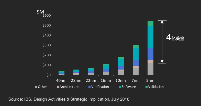
SoC (system-on-chip) designs integrate processors, analog and digital IP, memory, and interfaces on a single die. Since the 1990s SoCs have grown in functionality and transistor count, and modern SoC projects often require three to five years for a full development cycle. Given the high tapeout cost and irreversible schedule, verification must be exhaustive. In current SoC projects, simulation and verification frequently consume over 70% of total project time, and verification engineers often constitute more than 70% of the team. Extensive verification is required to find sufficient bugs before committing to tapeout.
Verification runs throughout the SoC design cycle
Verification activities start at project inception and continue through delivery and even after production. The flow is iterative and cross-disciplinary, and verification tasks often grow exponentially with time pressure. The major verification phases are outlined below.
1. Product planning
Verification planning begins early to define verification strategies, technical approaches, and debugging windows. SoC projects typically reuse mature IP to accelerate development, but IP selection must consider power, performance, security, cost, and interface compatibility. Early preparation of verification IP (VIP) and definition of check points across modules is important.
2. Architectural definition
SoC architecture definition covers functionality, communication protocols between IPs, and power/performance trade-offs. Two important verification activities at this stage are:
- Functional verification for different communication protocols to detect protocol-level bugs early at low cost.
- Prototyping to validate software-hardware interactions on an emulated hardware prototype. Early prototyping enables software and hardware co-design before silicon fabrication, reducing later integration risk and accelerating time to a usable system.
3. Pre-tapeout verification
Pre-tapeout verification is one of the most time- and resource-intensive phases. Individual IPs are validated in isolated environments, but system-level verification must ensure IPs and modules interoperate correctly. Common approaches include dynamic simulation and formal verification. Dynamic simulation requires a modeled test environment and waveform comparison, while formal methods build mathematical models and assertions to prove properties. As design complexity and maturity grow, pre-tapeout verification effort increases continuously.
4. Hardware acceleration (emulation and prototyping)
Hardware acceleration is a pre-tapeout technique that maps RTL to reconfigurable hardware to achieve speed-ups of thousands of times compared to RTL simulation, enabling full operating systems to boot on RTL-level designs in hours. Acceleration significantly improves verification throughput, but it reduces signal observability: signals to be observed must typically be defined before generating FPGA bitstreams, and recompilation can take many hours. To balance speed and observability, dedicated emulators are offered, but their cost and specialized hardware mean they are generally used by organizations with significant budgets.
5. Post-tapeout verification
Post-tapeout verification occurs after silicon fabrication but before mass production. Test lots are exercised in the lab to verify functionality, timing, performance, power, and physical robustness. Fixing bugs at this stage is expensive and sometimes infeasible. Some functional issues can be mitigated using firmware or microcode, but hardware fixes require respins and a new tapeout.
Verification challenges
Rising transistor counts, growing module counts, and increasing design complexity all demand more comprehensive verification. Different phases of chip design require different verification methods and tools, and hybrid approaches are common. Emerging markets such as 5G, big data, autonomous driving, and IoT have dramatically increased the number and variety of chips and placed higher demands on the SoC development cycle: how to perform more verification in less time? Two general strategies are improving tool scalability to make verification repeatable and reusable, and designing configurability into hardware and firmware so that fixes can be implemented without full respins.
1. Tool scalability
Scalability is key to tackling heavy verification loads, but many verification techniques lag behind the growth in SoC complexity. For example, while formal verification tools have advanced, they are increasingly used to target specific problems such as security or deadlock detection rather than as a universal solution. This specialization increases overall verification work since multiple complementary techniques must be applied rather than relying on a single scalable tool.
2. Lack of verification standards
Verification standards define what to verify and why. Traditional standards often rely on vague or incomplete requirements, leaving gray areas that are problematic for modern, cross-domain SoC designs. Processor vendors use instruction set simulators (ISS) as verification baselines, but SoCs include many heterogeneous modules and cross-module behavior that single-domain simulators cannot validate, complicating the establishment of meaningful verification baselines.
3. Widespread low-power techniques
Low-power design techniques are ubiquitous in IoT-era SoCs. Clock gating and power domain gating are commonly used to reduce static and dynamic power. Although standard languages exist to represent power intent for RTL simulation, low-power designs greatly increase verification complexity. It is common for a design to contain dozens of voltage domains and thousands of power modes; verification planning must ensure correct behavior across all modes, which significantly increases the verification burden.
4. Increasing security requirements
Information security requirements are at an all-time high. The proliferation of connected devices makes it difficult to enumerate potential attack surfaces and define verification objectives. Functional safety is another dimension: systems must fail safely in critical domains such as automotive and aerospace, and chips must be robust against transient events. These elevated security and safety requirements pose new verification challenges.
5. Hardware-software co-verification
In traditional PC environments hardware and software verification could be separated. Today the boundary is blurred: many SoC modules require firmware or software to exercise expected behaviors (for example, smartphones and automotive systems). Software development schedules must align with RTL progress, and software verification requires mature, stable, and fast hardware models. Joint verification must not only provide the necessary environment but also enable diagnosis of where and why errors occur across hardware and software layers.
Gaps in EDA tools developed in China
Over the past decade there has been progress in EDA technologies developed in China, but gaps remain. Key shortcomings include:
- A lack of core digital design tools covering the full digital design flow.
- Insufficient support for advanced process nodes; only a few tools support 14 nm, 7 nm, or 5 nm.
- A shortage of EDA systems for manufacturing and test that meet the needs of foundries and test houses.
- Missing core verification tools and integrated verification platforms; a complete EDA toolchain for verification is lacking.
Recent research indicates that EDA tools developed in China have a very small share of the Chinese market (around 0.8%). Observers note that the EDA market has intense international competition and limited margins, and that close collaboration between tools and advanced process design is required to solve critical “toolchain” challenges.
International EDA vendors currently offer comprehensive solutions across dynamic simulation, emulation/prototyping, and formal verification, and they continue to improve verification efficiency through methodology and adjacent technologies. In comparison, verification tool development in China is still at an early stage. Domestic EDA offerings have explored verification primarily in back-end implementation and chip test phases, but China-developed tool suites for digital integrated circuit verification during SoC design remain limited. Many Chinese chip design companies continue to rely on international EDA vendors for verification tools during SoC development.
Conclusion
Verification cannot prove the absence of all bugs; its role is to increase confidence to a point where the remaining risk is acceptable. Different SoC types require tailored verification strategies, tools, and environments. Large SoCs need complex flows that integrate multiple tools—virtual prototypes, simulators, emulators, and formal engines—in scalable and reusable ways.
Although verification tools developed in China are at an early stage and face a long road ahead, increasing SoC complexity and the resulting diversity of verification techniques may create opportunities for new entrants. The key challenges remain tool scalability, standards, power and security-aware verification, and hardware-software co-verification.