 ALLPCB


PCB trace impedance is a critical aspect of printed circuit board design, especially for high-speed and high-frequency applications. It determines how signals travel through the traces, ensuring signal integrity and minimizing interference. In this comprehensive guide, we’ll break down what PCB trace impedance is, the key factors affecting it, how to calculate it for single-ended and differential traces, and the best techniques to control it. Whether you're designing with microstrip or stripline configurations, understanding concepts like trace width, dielectric constant, and layer stackup will help you achieve optimal performance.
What is PCB Trace Impedance?
At its core, PCB trace impedance is the measure of opposition a trace offers to the flow of an alternating current (AC) signal. It combines resistance, inductance, and capacitance, forming what is known as characteristic impedance in an ideal transmission line. When the impedance of a trace matches the source and load, the signal travels without reflection, maintaining its integrity. Mismatches, however, can cause signal distortion, noise, or data loss, especially in high-speed circuits operating at frequencies above 100 MHz.
In this blog, we’ll dive deep into the factors that influence impedance, provide practical calculation methods, and share control techniques to ensure your designs meet performance requirements. Let’s explore this essential topic step by step.
Key Factors Affecting PCB Trace Impedance
Several physical and material properties impact the impedance of a PCB trace. Understanding these factors is the foundation of effective design.
1. Trace Width
The width of a PCB trace directly affects its impedance. Wider traces have lower impedance because they offer less resistance and inductance per unit length. For instance, a trace width of 10 mils might result in a characteristic impedance of 50 ohms on a standard FR-4 substrate, while narrowing it to 5 mils could increase the impedance to 75 ohms or more, depending on other factors. Adjusting trace width is often the simplest way to fine-tune impedance during design.
2. Dielectric Constant (Er)
The dielectric constant, often denoted as Er, is a property of the PCB substrate material (like FR-4, which typically has an Er of 4.2 to 4.5 at 1 GHz). It measures how much the material slows down an electric field compared to a vacuum. A higher dielectric constant reduces the impedance because it increases the capacitance between the trace and the ground plane. Choosing the right material is crucial for controlling impedance, especially in high-frequency designs.
3. Trace Thickness
The thickness of the copper trace also plays a role, though its impact is less significant than width. Thicker traces slightly lower impedance due to reduced resistance. Standard copper thicknesses are 1 oz/ft2 (about 1.4 mils) or 2 oz/ft2 (about 2.8 mils). While this factor is often fixed by manufacturing standards, it’s worth considering in precision designs.
4. Distance to Reference Plane (Height)
The height of the trace above or between reference planes (like ground or power planes) affects impedance through capacitance. A smaller distance increases capacitance, lowering impedance. For example, in a microstrip configuration, reducing the substrate height from 10 mils to 5 mils can significantly decrease the characteristic impedance if other parameters remain unchanged.
5. Layer Stackup
The arrangement of copper layers and insulating materials in a PCB, known as the layer stackup, determines how traces interact with each other and with reference planes. A well-designed stackup ensures consistent impedance across the board by maintaining uniform spacing and dielectric properties. For instance, embedding a trace between two ground planes in a stripline configuration offers better shielding and different impedance characteristics compared to a surface microstrip trace.
Types of PCB Trace Impedance: Single-Ended and Differential
PCB traces can carry signals in two primary configurations, each with unique impedance considerations.
Single-Ended Impedance
Single-ended traces carry a signal referenced to a ground plane. Their characteristic impedance, often targeted at 50 ohms for many high-speed applications, depends on the trace geometry and surrounding materials. Single-ended impedance is critical in applications like USB or HDMI, where signal integrity over a single conductor is paramount.
Differential Impedance
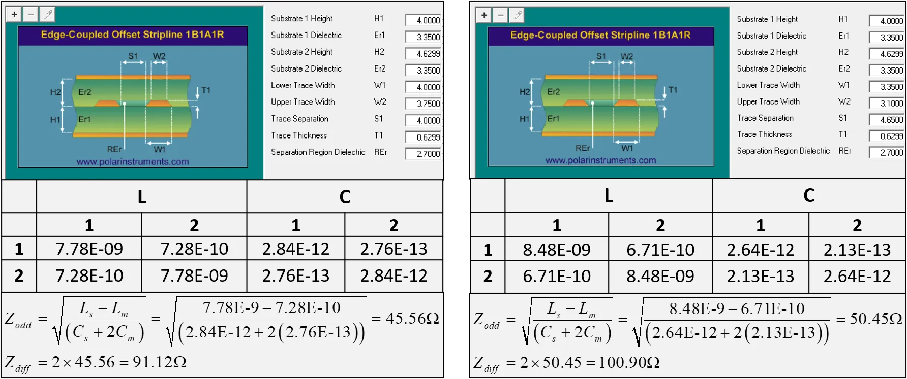
Differential traces involve two parallel traces carrying complementary signals, commonly used in high-speed interfaces like PCIe or Ethernet. The differential impedance, typically targeted at 90 to 100 ohms, is influenced not only by individual trace properties but also by the spacing between the pair. Closer spacing reduces differential impedance due to increased coupling between the traces.
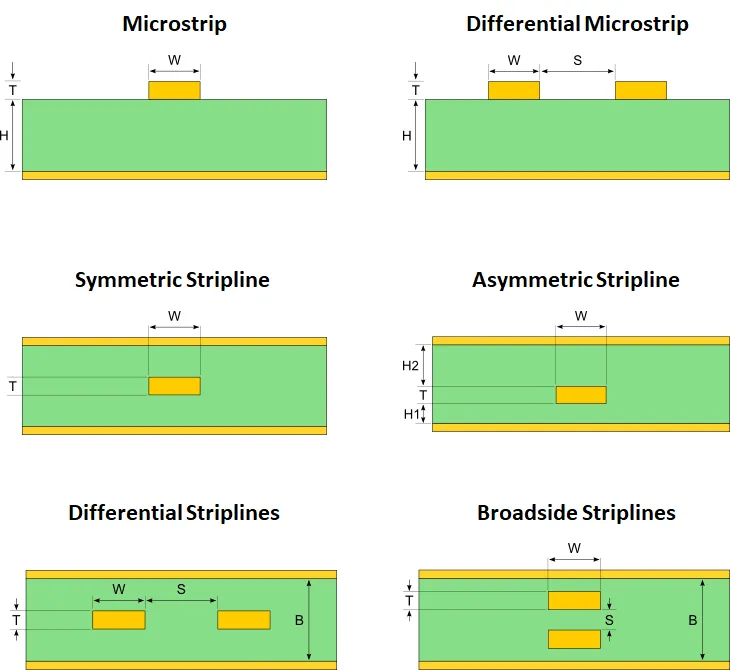
Microstrip vs. Stripline: Understanding Configurations
The placement of a trace relative to reference planes defines whether it’s a microstrip or stripline, each with distinct impedance characteristics.
Microstrip
Microstrip traces are located on the outer layers of a PCB, with a ground plane below them. They are easier to fabricate and inspect but are more susceptible to electromagnetic interference (EMI). Their impedance is influenced heavily by the dielectric constant of the substrate and the height above the ground plane. A typical microstrip trace might achieve 50 ohms with a width of 6 mils on a 10-mil thick FR-4 substrate.
Stripline
Stripline traces are embedded between two reference planes, offering better shielding from EMI. This configuration results in lower impedance for the same trace width compared to microstrip due to the dual-plane capacitance. Striplines are ideal for high-frequency signals but are harder to access for testing or rework.
How to Calculate PCB Trace Impedance
Calculating impedance is essential for matching traces to system requirements. While manual calculations using formulas are possible, modern tools simplify the process. Let’s explore both approaches.
Basic Impedance Formulas
For a microstrip trace, the characteristic impedance (Z0) can be approximated using the following simplified formula:
Z0 = (87 / √(Er + 1.41)) * ln(5.98 * H / (0.8 * W + T))
Where:
- Er = Dielectric constant of the substrate
- H = Height of the substrate (distance to ground plane)
- W = Trace width
- T = Trace thickness
For stripline, the formula adjusts for the dual-plane configuration, but it’s more complex due to additional variables. These formulas provide a starting point, though they assume ideal conditions and may deviate in real-world scenarios due to manufacturing tolerances.
For differential impedance, the calculation considers coupling between traces. A common target of 100 ohms for differential pairs often requires specific spacing, typically 2 to 3 times the trace width, depending on the stackup.
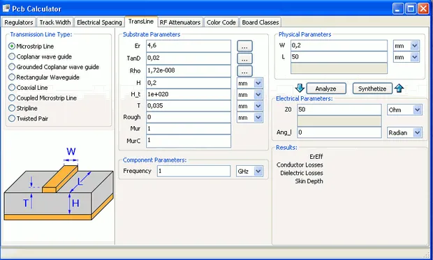
Using Impedance Calculators
Manual calculations are time-consuming and prone to error. Online tools and PCB design software offer impedance calculators that account for trace geometry, material properties, and layer stackup. These tools allow you to input parameters like trace width, substrate height, and dielectric constant to instantly compute single-ended or differential impedance. They often provide recommended values for achieving targets like 50 ohms or 100 ohms.
Control Techniques for PCB Trace Impedance
Achieving and maintaining the desired impedance requires careful design and manufacturing practices. Here are proven techniques to control impedance effectively.
1. Optimize Trace Width and Spacing
Adjusting the width of traces and the spacing between differential pairs is the most direct way to control impedance. Use design rules to ensure consistency across the board. For example, a 50-ohm single-ended trace might require a width of 6 mils, while a 100-ohm differential pair could need 5-mil traces with 8-mil spacing on a standard substrate.
2. Select Appropriate Materials
Choose substrate materials with a stable dielectric constant over the operating frequency range. FR-4 is common for general purposes, but high-frequency designs may benefit from materials like Rogers or Isola, which offer lower loss and tighter Er tolerances.
3. Design a Balanced Layer Stackup
A symmetrical layer stackup minimizes variations in impedance by ensuring uniform dielectric thickness and reference plane placement. Work with your PCB fabricator to define a stackup that supports your impedance targets, especially for multilayer boards with mixed microstrip and stripline traces.
4. Minimize Manufacturing Variations
Impedance can vary due to inconsistencies in trace etching, dielectric thickness, or copper weight. Specify tight tolerances for trace width (e.g., ±0.5 mils) and collaborate with your manufacturer to ensure controlled impedance processes are in place. Many fabricators offer impedance testing to verify that finished boards meet design specifications.
5. Use Simulation Tools
Before fabrication, simulate your design using electromagnetic field solvers or signal integrity analysis tools. These simulations predict impedance based on your layout and stackup, allowing you to make adjustments early in the design phase.
Why Controlling PCB Trace Impedance Matters
Proper impedance control is vital for maintaining signal integrity in modern electronics. High-speed signals, such as those in DDR memory or gigabit Ethernet, can suffer from reflections and crosstalk if impedance mismatches occur. These issues lead to data errors, increased EMI, and reduced system reliability. By focusing on factors like trace width, dielectric constant, and layer stackup, you can prevent these problems and ensure your PCB performs as intended.
For example, in a 5G communication board operating at 3 GHz, a mere 10% deviation from the target 50-ohm impedance could cause significant signal loss. Controlled impedance ensures that signals arrive at their destination with minimal distortion, supporting the performance of cutting-edge technologies.
Practical Tips for Designers
To wrap up, here are some actionable tips for managing PCB trace impedance in your projects:
- Start with a clear impedance target based on your application (e.g., 50 ohms for single-ended, 100 ohms for differential).
- Use design software with built-in impedance calculators to set trace dimensions early in the layout process.
- Communicate your impedance requirements and stackup details to your PCB manufacturer to avoid surprises during production.
- Consider environmental factors like temperature and humidity, which can slightly alter dielectric properties in sensitive designs.
- Test and validate your design with prototypes to confirm impedance values before full-scale production.
Conclusion
Understanding and controlling PCB trace impedance is a cornerstone of successful high-speed and high-frequency circuit design. By mastering factors like trace width, dielectric constant, and layer stackup, and by leveraging calculation tools and control techniques, you can ensure signal integrity and optimize performance. Whether you’re working with microstrip or stripline traces, or dealing with single-ended or differential impedance, a thoughtful approach to design and manufacturing will yield reliable results.
At ALLPCB, we’re committed to supporting engineers with the resources and expertise needed to tackle complex design challenges. With a focus on precision and quality, you can bring your innovative ideas to life with confidence. Dive into your next project with these insights on PCB trace impedance, and achieve designs that stand out in performance and reliability.


