ALLPCB


In PCB design for high voltage applications, copper foil thickness plays a critical role in ensuring safety, performance, and reliability. The thickness of the copper layer directly impacts the board's ability to handle high currents, resist heat, and maintain proper insulation to prevent breakdowns. For engineers working on high voltage systems, choosing the right copper thickness can mean the difference between a robust design and a catastrophic failure. In this blog, we’ll dive deep into why copper foil thickness matters, how it affects high voltage PCBs, and what factors you should consider during the design process.
Why Copper Foil Thickness Matters in PCB Design
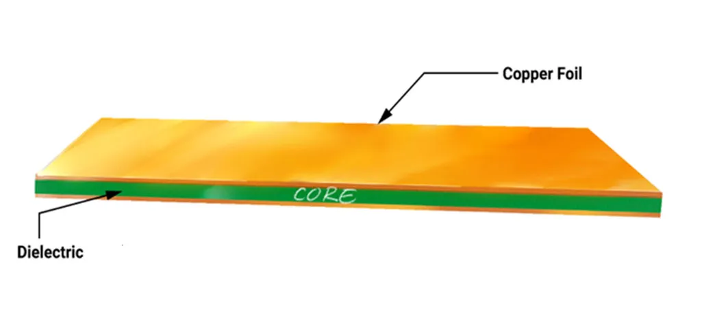
Copper foil is the conductive material in printed circuit boards (PCBs) that forms the traces, pads, and planes responsible for carrying electrical signals and power. In high voltage applications, where voltages can range from hundreds to thousands of volts, the demands on these copper layers are significantly higher than in standard electronics. The thickness of the copper foil—often measured in ounces per square foot (oz/ft2), where 1 oz/ft2 equals approximately 35 micrometers (μm) or 1.4 mils—determines how much current the board can carry, how much heat it can dissipate, and how well it can prevent electrical breakdowns.
In high voltage designs, insufficient copper thickness can lead to overheating, trace burnout, or even arcing between traces, which poses serious safety risks. On the other hand, using excessively thick copper can increase costs and make the PCB harder to manufacture. Striking the right balance is essential for engineers working on power supplies, electric vehicle systems, industrial equipment, and other high voltage projects.
Key Factors Influenced by Copper Foil Thickness in High Voltage Applications
Let’s break down the specific ways copper foil thickness impacts PCB performance in high voltage environments. Understanding these factors will help you make informed decisions during the design phase.
1. Current Carrying Capacity
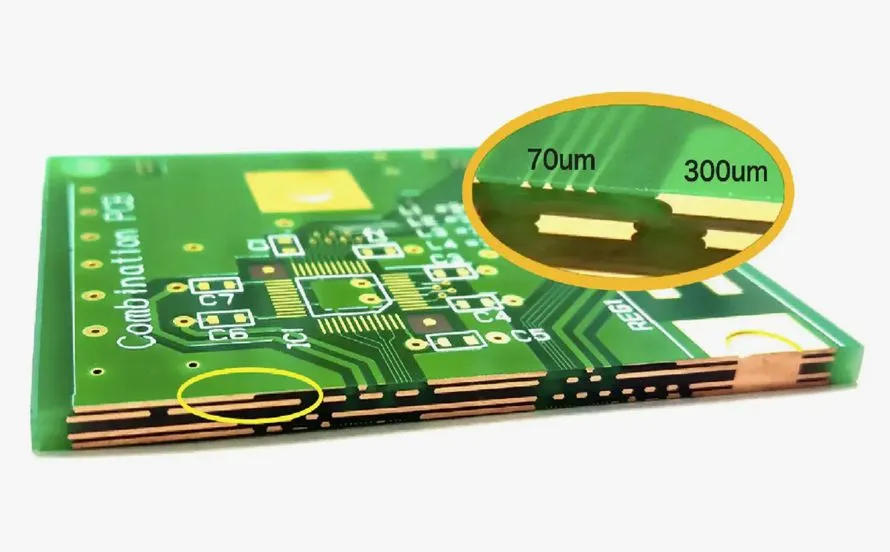
The primary role of copper foil in any PCB is to carry electrical current. In high voltage applications, the current levels are often high as well, especially in power electronics. The thicker the copper layer, the more current it can handle without overheating. For example, a 1 oz/ft2 copper layer can safely carry about 1-2 amps per 10 mils of trace width under typical conditions, but for high voltage systems with currents exceeding 10 amps, you might need 2 oz/ft2 (70 μm) or even 3 oz/ft2 (105 μm) copper to prevent thermal issues.
Thicker copper reduces the resistance of the traces, which minimizes voltage drops and power losses. This is especially important in high voltage designs where efficiency is a priority, such as in renewable energy systems or motor controllers.
2. Heat Dissipation and Thermal Management
High voltage often means high power, and high power generates heat. If the copper foil is too thin, it can’t dissipate heat effectively, leading to hotspots that degrade the PCB materials or cause component failure. Thicker copper layers have better thermal conductivity, allowing heat to spread out across the board and reducing the risk of thermal runaway.
For instance, in a high voltage power supply operating at 500V and 20A, a 1 oz/ft2 copper layer might overheat, while a 3 oz/ft2 layer can handle the load with a temperature rise of less than 20°C above ambient, staying within safe limits for most applications.
3. Dielectric Breakdown and Insulation
In high voltage applications, preventing dielectric breakdown—where electricity arcs through the insulating material between traces—is critical. While the PCB substrate (like FR-4) provides most of the insulation, the copper foil thickness indirectly affects spacing and clearance requirements. Thicker copper can sometimes allow for wider traces, which increases the distance between conductors and reduces the risk of arcing.
For example, at 1000V, the clearance between traces might need to be at least 3mm to prevent breakdown, depending on the material and environmental conditions. With thicker copper, you can design wider traces without sacrificing board space, improving safety.
4. Mechanical Strength and Durability
Thicker copper foil also adds mechanical strength to the PCB, making it more resistant to physical stress during manufacturing, assembly, or operation. In high voltage applications, where boards may be subject to vibration or thermal cycling (as in automotive or aerospace systems), this added durability can prevent cracks or delamination that could lead to failures.
How to Choose the Right Copper Foil Thickness for High Voltage PCBs
Selecting the appropriate copper thickness for your high voltage PCB design involves balancing performance, cost, and manufacturability. Here are the key steps to guide your decision.
1. Assess Voltage and Current Requirements
Start by calculating the expected voltage and current levels in your design. Use industry-standard charts or calculators to determine the minimum trace width and copper thickness needed to handle the current without exceeding a safe temperature rise (typically 10-20°C above ambient). For high voltage systems above 500V, consider starting with at least 2 oz/ft2 copper to ensure adequate current capacity and heat dissipation.
2. Consider Environmental Conditions
The operating environment affects how much heat your PCB can tolerate and how close traces can be without risking arcing. High humidity or altitude can lower the dielectric strength of air, requiring greater spacing or thicker insulation. Thicker copper can help by allowing wider traces, but you may also need to pair it with a high-quality substrate material rated for high voltage, such as polyimide.
3. Factor in Manufacturing Constraints
While thicker copper (e.g., 3 oz/ft2 or more) is beneficial for high voltage designs, it can complicate manufacturing. Etching finer traces becomes harder with thicker copper, and the cost of materials increases. Work with your PCB fabrication partner to ensure they can handle the desired thickness while meeting your design tolerances.
4. Account for Cost vs. Performance
Thicker copper foil increases the cost of the PCB, both in terms of raw materials and manufacturing complexity. For high voltage applications, safety and reliability often justify the expense, but if your design operates at the lower end of the high voltage spectrum (e.g., 100-300V), a 1.5 oz/ft2 or 2 oz/ft2 layer might be sufficient, saving on cost without compromising performance.
Common Copper Foil Thicknesses for High Voltage Applications
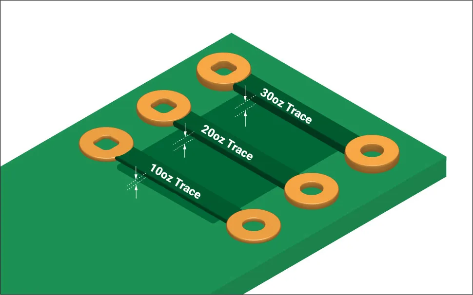
Copper foil thickness is typically specified in ounces per square foot, with standard options ranging from 0.5 oz/ft2 to 4 oz/ft2 or more for specialized applications. Here’s a breakdown of common thicknesses and their suitability for high voltage designs:
- 0.5 oz/ft2 (17.5 μm): Used in low-power, signal-only PCBs. Not suitable for high voltage due to limited current capacity and heat dissipation.
- 1 oz/ft2 (35 μm): The most common thickness for standard PCBs. May work for high voltage designs with low current (under 2-3A) and proper spacing, but often insufficient for power applications.
- 2 oz/ft2 (70 μm): A good starting point for many high voltage applications, offering better current handling (up to 5-10A per trace, depending on width) and thermal performance.
- 3-4 oz/ft2 (105-140 μm): Ideal for high voltage, high current designs like power converters or electric vehicle systems, where currents exceed 10A and heat dissipation is critical.
For extreme high voltage applications (above 1000V) or very high currents, some designs use even thicker copper or incorporate heavy copper layers (up to 10 oz/ft2 or 350 μm), though these are less common and require specialized manufacturing processes.
Design Tips for High Voltage PCBs with Optimal Copper Thickness
Beyond selecting the right copper foil thickness, here are some practical design tips to ensure your high voltage PCB performs reliably:
- Increase Trace Spacing: Follow industry standards like IPC-2221 for clearance and creepage distances based on your voltage levels. For 500V, a minimum clearance of 2.5mm is often recommended, increasing to 5mm or more at 1000V.
- Use Wider Traces: Wider traces reduce resistance and heat buildup. Pair this with thicker copper for maximum current capacity.
- Incorporate Thermal Vias: Add vias to transfer heat from copper layers to other parts of the board or to a heat sink, especially in high power designs.
- Choose High Voltage Materials: Pair thick copper with substrates that have high dielectric strength, such as FR-4 with a high CTI (Comparative Tracking Index) rating or specialized materials like polyimide.
- Test for Reliability: Simulate your design under worst-case conditions to verify that the copper thickness and trace layout can handle the voltage, current, and thermal load without failure.
Challenges with Thick Copper in High Voltage PCB Design
While thicker copper foil offers clear benefits for high voltage applications, it also introduces some challenges that engineers must address:
- Manufacturing Limitations: Etching precise traces becomes more difficult with copper thicker than 2 oz/ft2, potentially limiting how fine your design can be.
- Increased Weight: Thicker copper adds weight to the PCB, which may be a concern in applications like aerospace where every gram counts.
- Higher Costs: The raw material and processing costs rise with copper thickness, impacting the overall budget of your project.
- Layer Bonding Issues: In multilayer PCBs, very thick copper can create uneven surfaces, making it harder to bond layers together without voids or defects.
Work closely with your PCB manufacturer to understand their capabilities and limitations when specifying thicker copper for high voltage designs.
Conclusion: Balancing Copper Thickness for High Voltage Success
Copper foil thickness is a cornerstone of effective PCB design for high voltage applications. It influences everything from current carrying capacity and heat dissipation to insulation safety and mechanical durability. By carefully assessing your project’s voltage, current, and environmental requirements, you can select the optimal copper thickness—whether it’s 2 oz/ft2 for moderate high voltage systems or 4 oz/ft2 for demanding power electronics.
Remember that thicker copper isn’t just about performance; it’s also about safety. High voltage designs carry inherent risks, and the right copper thickness helps mitigate those risks by preventing overheating, arcing, and breakdowns. Pair this with smart design practices like proper trace spacing and high-quality materials, and you’ll be well on your way to creating reliable, efficient high voltage PCBs for any application.
At ALLPCB, we’re committed to supporting engineers with the resources and expertise needed to bring high voltage designs to life. Whether you’re working on industrial equipment, renewable energy systems, or automotive electronics, understanding the role of copper foil thickness is the first step toward success.