 ALLPCB


In the world of printed circuit board (PCB) design and manufacturing, copper balancing plays a crucial role in ensuring the quality, reliability, and performance of the final product. But what exactly is copper balancing, and why is it so important in PCB fabrication and component assembly? Simply put, copper balancing refers to the even distribution of copper across the layers of a PCB to prevent issues like warping, uneven plating, and poor signal integrity during the manufacturing process. In this blog, we’ll dive deep into the significance of copper balancing, how it impacts PCB design, fabrication, and assembly, and why it’s a key factor for engineers to consider.
Whether you’re an electronics engineer or a hobbyist, understanding copper balancing can help you create better designs and avoid costly manufacturing defects. Let’s explore this topic step by step, breaking down its role in the PCB manufacturing process and offering practical insights for achieving optimal results.
What Is Copper Balancing in PCB Design?
Copper balancing is the practice of distributing copper evenly across the layers of a PCB during the design and fabrication stages. In a typical PCB, copper is used to form conductive traces, pads, and planes that carry electrical signals and power between components. However, if the copper is unevenly distributed—say, with a dense copper area on one side of the board and little to no copper on the other—it can lead to mechanical and electrical issues.
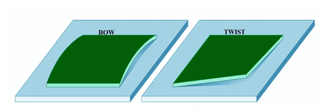
During PCB fabrication, uneven copper distribution can cause the board to warp or twist due to differences in thermal expansion and contraction. This not only affects the structural integrity of the board but also complicates component assembly, as misaligned boards can lead to soldering defects. Additionally, unbalanced copper can result in inconsistent plating during the manufacturing process, leading to variations in trace thickness and potential weak spots in the circuit.
For engineers working on PCB design, achieving copper balance means strategically placing copper features like traces, ground planes, and dummy fills (non-functional copper areas) to ensure uniformity. This step is critical for maintaining the board’s flatness, improving manufacturability, and ensuring reliable performance in the final product.
Why Is Copper Balancing Important in PCB Fabrication?
Copper balancing is a vital aspect of PCB fabrication because it directly impacts the board’s quality and yield during production. Here are some key reasons why it matters:
1. Prevents Warping and Twisting
During the fabrication process, PCBs are exposed to high temperatures and chemical processes like etching and plating. If copper is unevenly distributed, the board can experience uneven stress, leading to warping or twisting. For instance, a board with a heavy copper ground plane on one side and sparse traces on the other may bend during lamination or soldering. Warped boards are difficult to assemble and can fail quality checks, increasing production costs.
2. Ensures Uniform Plating
In PCB fabrication, copper plating is used to build up the thickness of traces and vias. If the copper distribution is uneven, the electroplating process can result in inconsistent copper thickness across the board. Areas with more copper may attract more plating, while areas with less copper may end up under-plated. This imbalance can weaken connections and affect the board’s electrical performance. Proper copper balancing ensures uniform plating, maintaining consistent trace impedance—often critical for high-speed designs where impedance values need to be within 5-10% of the target (e.g., 50 ohms for many RF applications).
3. Improves Thermal Management
Copper conducts heat as well as electricity, so balanced copper distribution helps manage thermal dissipation during operation. Without balance, localized hotspots can form in areas with dense copper, potentially damaging components or degrading performance. By spreading copper evenly, heat is distributed more uniformly, reducing the risk of thermal stress.
How Copper Balancing Affects Component Assembly
Beyond fabrication, copper balancing plays a significant role in the component assembly stage of the PCB manufacturing process. Here’s how it influences this critical step:
1. Ensures Flatness for Soldering
During component assembly, a flat PCB is essential for accurate placement and soldering of components. Surface-mount technology (SMT) machines, for example, rely on a perfectly level board to place components with precision. If the board is warped due to unbalanced copper, components may not align correctly with their pads, leading to poor solder joints or even complete assembly failures. Balanced copper distribution minimizes warping, ensuring a smooth assembly process.
2. Reduces Risk of Tombstoning
Tombstoning is a common defect in SMT assembly where one end of a component lifts off the pad during reflow soldering, resembling a tombstone. This issue can occur due to uneven heating caused by imbalanced copper distribution. For instance, if one pad has significantly more copper than the other, it may heat up faster, causing uneven solder melting. Copper balancing helps maintain uniform thermal profiles across the board, reducing the likelihood of such defects.
3. Supports High-Density Designs
In modern electronics, PCBs often feature high-density layouts with tightly packed components. Uneven copper can exacerbate signal integrity issues in these designs, especially for high-speed signals where controlled impedance is critical. Balanced copper distribution, including the use of ground planes and proper trace spacing, helps maintain signal integrity during assembly and operation, ensuring that data rates—often in the range of 1-10 Gbps for high-speed applications—are not compromised.
Techniques for Achieving Copper Balancing in PCB Design
Now that we understand the importance of copper balancing in PCB fabrication and component assembly, let’s look at some practical techniques to achieve it during the design phase.
1. Use of Copper Thieving
Copper thieving involves adding non-functional copper patterns, often in the form of small squares or dots, to areas of the board with low copper density. These “thieves” balance out the copper distribution, ensuring uniform plating and reducing the risk of warping. Thieving is especially useful in outer layers where large empty spaces might otherwise exist.
2. Incorporate Hatch Patterns
For large copper planes, such as ground or power planes, using a hatched or crosshatched pattern instead of a solid plane can help balance copper density. Hatching reduces the overall copper coverage while still providing the necessary electrical functionality, making it easier to achieve balance with other layers.
3. Symmetrical Layer Stack-Up
In multilayer PCBs, copper balancing isn’t just about individual layers but also about the entire stack-up. Designing a symmetrical stack-up, where copper distribution is mirrored across corresponding layers, helps maintain overall balance. For example, if layer 1 has a dense copper area, layer 8 (in an 8-layer board) should have a similar density to prevent uneven stress.
4. Dummy Fills and Unused Pads
Adding dummy fills—unused copper areas or pads—can help balance copper in sparse regions of the board. These fills don’t connect to any circuit but serve to even out the copper density, aiding in fabrication and assembly processes.
Challenges in Copper Balancing for PCB Manufacturing
While copper balancing is essential, it’s not always straightforward to implement. Here are some common challenges engineers face during the PCB manufacturing process:
1. Design Constraints
In high-density or compact designs, there may be limited space to add dummy fills or thieving patterns. Engineers must balance the need for copper uniformity with the functional requirements of the circuit, which can be a delicate trade-off.
2. Signal Integrity Concerns
Adding extra copper for balancing purposes can sometimes interfere with signal integrity, especially in high-frequency designs. For instance, excessive copper near sensitive traces might introduce parasitic capacitance, altering impedance values (e.g., shifting from a target of 50 ohms to 55 ohms). Careful planning and simulation are needed to avoid such issues.
3. Manufacturing Limitations
Not all fabrication processes can accommodate intricate copper balancing techniques. For example, very fine thieving patterns may be difficult to etch accurately, leading to inconsistencies. Working closely with your manufacturing partner during the design phase can help address these limitations.
Best Practices for Copper Balancing in PCB Fabrication
To ensure successful copper balancing in PCB fabrication and component assembly, consider the following best practices:
- Collaborate Early with Manufacturers: Share your design files with your fabrication partner during the initial stages to get feedback on copper distribution and stack-up symmetry.
- Use Design Software Tools: Leverage PCB design software with built-in features for copper balancing, such as automatic thieving or density checks, to identify potential issues before fabrication.
- Test and Iterate: For critical projects, consider prototyping with different copper balancing techniques to evaluate their impact on board flatness and performance.
- Prioritize Signal Requirements: Always ensure that copper balancing efforts don’t compromise the electrical performance of the board, especially for high-speed or RF applications.
The Impact of Copper Balancing on Overall PCB Performance
Copper balancing doesn’t just affect fabrication and assembly—it also has a long-term impact on the performance and reliability of the PCB in real-world applications. A well-balanced board is less likely to suffer from mechanical failures like cracking or delamination over time. It also ensures consistent electrical performance, with stable impedance and minimal signal loss, which is crucial for applications like telecommunications, automotive systems, and medical devices.
For high-speed designs, balanced copper helps maintain signal integrity by reducing crosstalk and electromagnetic interference (EMI). In power electronics, it supports efficient current distribution, preventing voltage drops and overheating. By investing time in copper balancing during the design phase, engineers can significantly enhance the durability and functionality of their PCBs.
Conclusion: Mastering Copper Balancing for Better PCBs
Copper balancing is a fundamental yet often overlooked aspect of PCB design, fabrication, and component assembly. By ensuring even copper distribution across layers, engineers can prevent manufacturing defects, improve assembly accuracy, and enhance the overall performance of their boards. From preventing warping and ensuring uniform plating to supporting high-speed signal integrity, the benefits of copper balancing are clear.
As you work on your next PCB project, keep copper balancing in mind during the design phase. Use techniques like thieving, hatching, and symmetrical stack-ups to achieve uniformity, and collaborate with your manufacturing partner to address any challenges. With careful planning and attention to detail, you can create high-quality PCBs that meet the demands of even the most complex applications.
At ALLPCB, we’re committed to supporting engineers with the tools and expertise needed for successful PCB fabrication and assembly. By prioritizing copper balancing, you’re taking a key step toward building reliable, high-performing boards that stand the test of time.


