ALLPCB


Introduction
Thermal management plays a critical role in the design of printed circuit boards, especially when dealing with thick PCBs used in high power and high density applications. Thick PCBs, often employed in industries like automotive, aerospace, and industrial electronics, face unique challenges due to increased layer counts and material thickness, which can exacerbate heat buildup. Without proper thermal simulation, these designs risk overheating, component failure, and reduced reliability. Thermal simulation for PCBs provides engineers with a predictive tool to analyze heat distribution, identify hotspots, and optimize cooling strategies before manufacturing begins. This article explores the significance of PCB thermal analysis, the underlying principles of heat simulation, and best practices for ensuring efficient thermal design in thick PCB layouts. Understanding these concepts is essential for electrical engineers aiming to create robust and reliable electronic systems.
What Is Thermal Simulation in PCB Design and Why It Matters
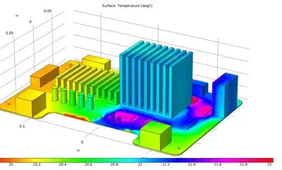
Thermal simulation for PCBs involves the use of specialized software to model and predict how heat flows through a circuit board during operation. This process, often referred to as PCB heat simulation, allows engineers to visualize temperature gradients, identify potential overheating areas, and assess the effectiveness of cooling mechanisms. In thick PCB designs, where multiple layers and dense component placement amplify thermal challenges, such simulations are indispensable. These boards often handle high currents or support power intensive components, leading to significant heat generation that must be dissipated effectively.
The importance of PCB thermal analysis lies in its ability to prevent costly design failures. Overheating can degrade component performance, cause material delamination, or lead to complete system shutdowns. By conducting thermal simulations early in the design phase, engineers can make informed decisions about material selection, layer stackup, and component placement to enhance heat dissipation. This proactive approach reduces the need for redesigns, shortens development cycles, and ensures compliance with industry standards for reliability and safety. For thick PCBs, where thermal mass is greater, simulation becomes even more critical to achieving a balanced and efficient design.
Technical Principles of Thermal Simulation in PCB Design
Thermal simulation in PCB design relies on fundamental principles of heat transfer, including conduction, convection, and radiation. Conduction is the primary mode of heat transfer within the solid materials of a PCB, such as copper traces, vias, and dielectric layers. The efficiency of conduction depends on the thermal conductivity of the materials used and the design of thermal pathways like vias or planes. Convection occurs when heat is transferred from the PCB surface to the surrounding air or a cooling medium, often aided by fans or heatsinks. Radiation, though less significant in most PCB applications, involves heat loss through electromagnetic waves and can be relevant in high temperature environments.
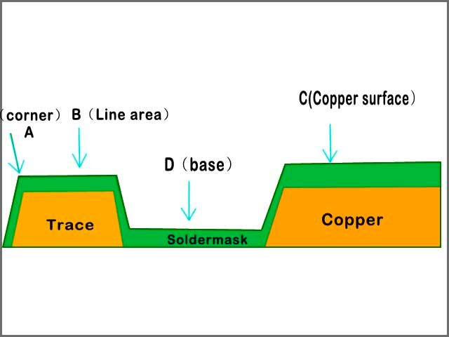
In thick PCBs, the increased number of layers and overall thickness can impede heat dissipation, creating localized hotspots. PCB cooling simulation models these heat transfer mechanisms using numerical methods like finite element analysis or computational fluid dynamics. These simulations account for factors such as component power dissipation, ambient temperature, and airflow conditions to predict temperature profiles across the board. Engineers input parameters like material properties and boundary conditions into thermal design software to generate accurate results. Standards such as IPC-2152, which provides guidelines for current carrying capacity and temperature rise in PCB traces, often inform these simulations to ensure realistic outcomes.
Another key aspect is the role of thermal vias and copper planes in managing heat. Thermal vias act as conduits to transfer heat from surface layers to inner layers or external heatsinks, while copper planes spread heat across larger areas. Simulating these elements helps determine their optimal placement and density. Without proper analysis, thick PCBs risk uneven heat distribution, which can stress components or cause warpage.
Challenges Specific to Thick PCB Thermal Management
Thick PCBs, typically defined as boards with more than six layers or a thickness exceeding 2.4 millimeters, present unique thermal challenges. The increased material volume acts as a thermal mass, slowing down heat dissipation and making it harder to maintain uniform temperatures. High layer counts also mean more embedded components or power planes, which can generate heat deep within the board where natural convection is limited. Additionally, the dielectric materials used in thick PCBs often have lower thermal conductivity, further complicating heat management.
PCB thermal analysis must account for these factors to prevent issues like thermal expansion mismatches between layers, which can lead to mechanical stress or delamination. Standards such as IPC-6012E, which outlines performance specifications for rigid printed boards, emphasize the need for robust thermal design to ensure structural integrity under operating conditions. Simulation helps engineers evaluate how heat accumulates in critical areas and whether additional cooling solutions, such as forced air or liquid cooling, are necessary. Neglecting these challenges can result in reduced lifespan of components or failure to meet regulatory requirements for thermal performance.
Best Practices for Thermal Simulation in Thick PCB Design
Implementing effective thermal simulation requires a structured approach to ensure accurate results and actionable insights. Below are key best practices for electrical engineers working on thick PCB designs using PCB heat simulation and thermal design software.
- Define Accurate Input Parameters: Start by gathering precise data on component power dissipation, material thermal properties, and environmental conditions. This includes ambient temperature, airflow rates, and mounting configurations. Accurate inputs lead to reliable simulation outcomes.
- Select Appropriate Materials: Choose substrates and laminates with higher thermal conductivity when possible, especially for thick PCBs. Simulation can help compare different material options to balance cost and performance.
- Optimize Component Placement: Place heat generating components away from each other and near effective cooling paths. Use PCB cooling simulation to test various layouts and identify the most thermally efficient arrangement.
- Incorporate Thermal Vias and Planes: Strategically place thermal vias and copper planes to create low resistance paths for heat transfer. Simulate different configurations to determine the optimal number and spacing of vias.
- Validate with Standards: Align simulation parameters with industry guidelines such as IPC-2152 for trace temperature rise and IPC-A-600K for board acceptability criteria. This ensures designs meet established benchmarks for thermal reliability.
- Iterate and Test Designs: Run multiple simulations to explore different scenarios, such as varying ambient temperatures or power loads. Use results to refine the design before prototyping to minimize physical testing costs.
Additionally, consider integrating passive and active cooling solutions based on simulation findings. For instance, if hotspots persist near critical components, adding heatsinks or fans might be necessary. PCB thermal analysis can quantify the impact of these solutions, helping engineers make data driven decisions.
Tools and Methods for Effective PCB Thermal Analysis
Thermal design software plays a vital role in conducting accurate simulations for thick PCBs. These tools typically offer features like 3D modeling, transient analysis, and integration with electrical design data to provide comprehensive thermal insights. Engineers can simulate steady state conditions to understand long term heat distribution or transient states to analyze short term thermal spikes during power surges.
Common methods in PCB cooling simulation include setting up boundary conditions that mimic real world environments and defining heat sources based on component specifications. The software then solves heat transfer equations to predict temperature profiles and airflow patterns. Some tools also allow coupling of thermal and electrical simulations to assess how temperature affects circuit performance, which is particularly useful for power dense thick PCBs.
While specific software names are outside the scope of this discussion, it is worth noting that adhering to industry standards during simulation setup is crucial. For example, JEDEC J-STD-020E provides guidelines for moisture and reflow sensitivity, which can influence thermal behavior during manufacturing and should be considered in simulation models.
Conclusion
Thermal simulation is a cornerstone of effective thick PCB design, offering electrical engineers the ability to predict and mitigate heat related issues before they impact performance. By leveraging PCB thermal analysis, designers can optimize material choices, component layouts, and cooling strategies to ensure reliability in demanding applications. Understanding the principles of heat transfer and applying best practices through simulation tools allows for the creation of robust boards that withstand thermal stresses. As electronic systems continue to grow in complexity, especially in thick PCB applications, the role of thermal design software and heat simulation becomes ever more critical. Prioritizing these processes not only enhances product longevity but also aligns with industry standards for quality and safety.
FAQs
Q1: How does thermal simulation for PCB design improve reliability in thick boards?
A1: Thermal simulation for PCB design helps identify hotspots and uneven heat distribution in thick boards, which often have high thermal mass. By predicting temperature profiles, engineers can adjust layouts, add thermal vias, or select better materials to prevent overheating. This reduces the risk of component failure and ensures long term reliability under high power conditions.
Q2: What factors should be considered during PCB thermal analysis for thick designs?
A2: During PCB thermal analysis, engineers must consider component power dissipation, material thermal conductivity, layer stackup, and ambient conditions. Thick designs require special attention to heat trapped in inner layers. Simulating these factors helps optimize cooling paths and prevents issues like thermal expansion or delamination.
Q3: Why is PCB cooling simulation critical for high power applications?
A3: PCB cooling simulation is essential for high power applications because it models how heat dissipates under intense operating conditions. Thick PCBs in such scenarios face increased heat generation, risking component damage. Simulation allows testing of cooling solutions like heatsinks or airflow to maintain safe temperatures.
Q4: How does thermal design software aid in thick PCB development?
A4: Thermal design software provides detailed modeling of heat flow in thick PCBs, enabling engineers to visualize temperature gradients and test design changes virtually. It supports iterative optimization of layouts and materials, reducing prototyping costs and ensuring thermal performance aligns with operational requirements.
References
IPC-2152 — Standard for Determining Current Carrying Capacity in Printed Board Design. IPC, 2009.
IPC-6012E — Qualification and Performance Specification for Rigid Printed Boards. IPC, 2020.
IPC-A-600K — Acceptability of Printed Boards. IPC, 2020.
JEDEC J-STD-020E — Moisture/Reflow Sensitivity Classification for Nonhermetic Surface Mount Devices. JEDEC, 2014.