 ALLPCB


In the world of electronics, printed circuit boards (PCBs) are the backbone of nearly every device we use. However, the process of manufacturing PCBs, including advanced techniques like via-in-pad, can have a significant environmental impact. How can we make PCB manufacturing more sustainable? The answer lies in adopting eco-friendly practices, using greener materials, and optimizing processes to reduce waste and energy consumption. In this blog, we’ll explore the environmental challenges of via-in-pad PCB manufacturing and share actionable strategies for creating sustainable electronics with a focus on green PCB solutions.
What Is Via-in-Pad PCB Manufacturing?
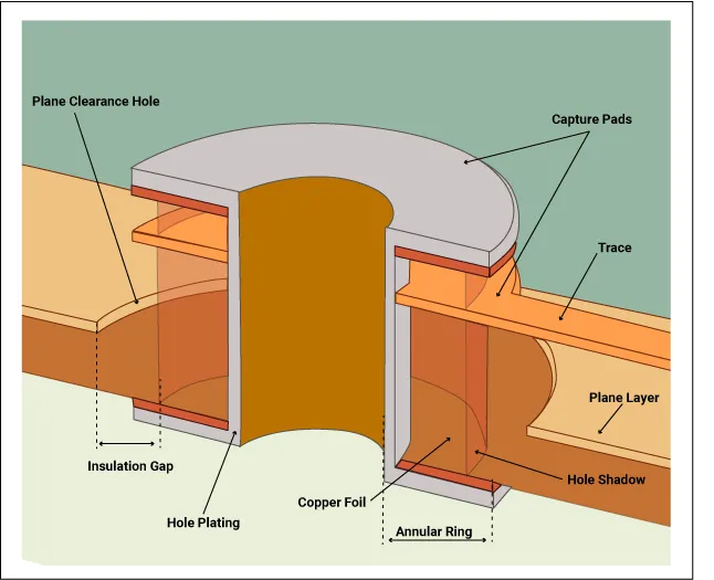
Via-in-pad is a specialized PCB design technique where vias—small holes that connect different layers of a circuit board—are placed directly within the solder pads of surface-mounted components. This approach is often used in high-density interconnect (HDI) designs to save space and improve signal integrity. It’s especially common in compact devices like smartphones and wearables, where every millimeter of board space matters.
While via-in-pad offers technical advantages, such as reduced parasitic inductance and better thermal management, the manufacturing process can be resource-intensive. It often requires additional steps like via filling with conductive or non-conductive materials, precise drilling, and plating, all of which consume energy and materials. Understanding these processes is the first step in addressing their environmental impact and moving toward sustainable electronics.
The Environmental Impact of PCB Manufacturing
PCB manufacturing, including via-in-pad techniques, has several environmental consequences that affect air, water, and soil quality. Let’s break down the key areas of concern:
1. Energy Consumption
The production of PCBs is an energy-intensive process. From drilling and etching to plating and lamination, each step requires significant electricity, often sourced from non-renewable fossil fuels. For via-in-pad designs, the additional steps of via filling and precise alignment increase energy demands further. Studies suggest that the electronics manufacturing sector accounts for a substantial portion of industrial energy use, contributing to greenhouse gas emissions.
2. Chemical Usage and Waste
Chemicals play a major role in PCB production. Etching solutions, plating chemicals, and solvents are used to create circuit patterns and protect board surfaces. In via-in-pad manufacturing, extra chemicals may be needed for filling vias or ensuring proper adhesion. If not managed properly, these chemicals can contaminate water sources and harm ecosystems. Improper disposal of chemical waste remains a challenge in many manufacturing regions.
3. Material Waste
PCB manufacturing generates material waste, including scrap copper, fiberglass, and epoxy resins. Via-in-pad designs, due to their complexity, often result in higher rates of defective boards during production, leading to more waste. Additionally, the non-recyclable nature of some traditional PCB materials makes it difficult to recover and reuse resources, contributing to landfill accumulation.
4. Water Usage
Water is used extensively in PCB manufacturing for rinsing boards, cooling equipment, and processing chemicals. The via-in-pad process, with its extra plating and cleaning steps, can increase water consumption. Without proper treatment, wastewater containing heavy metals like copper and lead can pollute local water bodies, posing risks to human and environmental health.
Challenges Specific to Via-in-Pad Manufacturing
While via-in-pad technology offers design benefits, it introduces unique environmental challenges due to its complexity. For instance, the need for precise micro-drilling and via filling often results in higher energy use compared to standard PCB designs. The materials used for filling vias, such as epoxy or conductive pastes, may not always be eco-friendly, and their application can generate additional waste.
Moreover, the high-density nature of via-in-pad boards often means they are used in short-lifecycle products like consumer electronics. This contributes to electronic waste (e-waste) when devices are discarded, as recovering materials from complex HDI boards is technically challenging and costly. Addressing these issues requires innovative approaches to make via-in-pad manufacturing align with green PCB principles.
Toward Sustainable Electronics: Eco-Friendly PCB Practices
The good news is that the electronics industry is increasingly recognizing the need for sustainability. By adopting eco-friendly PCB practices, manufacturers can reduce the environmental impact of via-in-pad and other PCB production methods. Below are some actionable strategies for creating greener electronics:
1. Use of Eco-Friendly Materials
Traditional PCB substrates like FR-4 are made from fiberglass and epoxy resins, which are difficult to recycle. Switching to biodegradable or recyclable materials can significantly lower the environmental footprint. For example, some innovative substrates are made from natural fibers or compostable polymers, offering a sustainable alternative without compromising performance. While these materials may not yet be widely used in via-in-pad designs, ongoing research is making them more viable for high-density applications.
Additionally, opting for lead-free solders and halogen-free laminates reduces the release of toxic substances during manufacturing and disposal. These choices align with global regulations like RoHS (Restriction of Hazardous Substances) and support the goal of sustainable electronics.
2. Energy-Efficient Manufacturing Processes
Reducing energy consumption is critical for green PCB production. Manufacturers can invest in energy-efficient equipment and optimize production workflows to minimize power usage. For via-in-pad manufacturing, using advanced laser drilling technology instead of mechanical drilling can lower energy needs while achieving precise results. Furthermore, sourcing electricity from renewable sources like solar or wind can cut down on carbon emissions associated with PCB production.
3. Waste Reduction and Recycling
Minimizing waste during PCB manufacturing starts with better design practices. By optimizing layouts to reduce material offcuts and improving quality control to lower defect rates, manufacturers can decrease scrap. For via-in-pad boards, simulation tools can help predict and prevent manufacturing errors, reducing the number of unusable boards.
Recycling programs are also essential. Setting up systems to recover copper and other metals from defective or end-of-life PCBs can conserve resources. While recycling complex via-in-pad boards is challenging due to their multilayer structure, emerging technologies are making it possible to separate and reuse components effectively.
4. Water Conservation and Treatment
Water usage in PCB manufacturing can be reduced by implementing closed-loop systems that recycle rinse water. For via-in-pad processes, which require additional cleaning steps, advanced filtration technologies can remove contaminants from wastewater, allowing it to be reused. Proper treatment of wastewater before discharge ensures that harmful chemicals and metals do not enter the environment, protecting local ecosystems.
Benefits of Adopting Green PCB Practices
Transitioning to sustainable electronics through green PCB practices offers multiple benefits, both for the environment and for businesses involved in PCB manufacturing:
- Reduced Environmental Footprint: By using eco-friendly materials and processes, manufacturers can lower emissions, conserve resources, and minimize pollution.
- Compliance with Regulations: Adhering to environmental standards like RoHS and REACH (Registration, Evaluation, Authorization, and Restriction of Chemicals) helps avoid legal penalties and builds trust with customers.
- Cost Savings: Energy-efficient processes and waste reduction can lead to long-term savings on raw materials and utility costs, even if initial investments are required.
- Enhanced Brand Reputation: Companies that prioritize sustainability attract environmentally conscious customers and partners, strengthening their position in the market.
Innovations Driving Sustainable Via-in-Pad Manufacturing
The push for sustainability is driving innovation in via-in-pad PCB manufacturing. For instance, advancements in conductive inks and pastes for via filling are reducing the need for energy-intensive plating processes. Some manufacturers are exploring water-based via-fill materials that break down more easily at the end of a product’s life, aiding recycling efforts.
Digital twin technology is another game-changer. By creating virtual models of PCB designs and manufacturing processes, engineers can simulate via-in-pad production to identify inefficiencies and reduce errors before physical production begins. This cuts down on material waste and energy use, supporting the goal of sustainable electronics.
Additionally, the rise of modular electronics design—where components can be easily replaced or upgraded—reduces the need to discard entire boards, including those with via-in-pad structures. While not yet widespread, these innovations show promise for a greener future in PCB manufacturing.
How Manufacturers Can Lead the Way in Green PCB Production
For manufacturers, taking a proactive approach to sustainability in PCB production, including via-in-pad techniques, is essential. Start by conducting an environmental audit of current processes to identify areas for improvement, such as high energy use or excessive chemical waste. Partnering with suppliers who prioritize eco-friendly materials can also make a big difference in reducing the overall impact.
Investing in employee training ensures that staff are aware of sustainable practices and know how to implement them effectively. Finally, transparency in supply chains—such as sharing information about material sourcing and waste management—builds trust with customers and demonstrates a commitment to environmental responsibility.
Conclusion: Building a Sustainable Future with Eco-Friendly PCBs
The environmental impact of via-in-pad PCB manufacturing is a pressing concern, but it’s one that the industry can address through innovation and commitment to sustainability. By focusing on eco-friendly materials, energy-efficient processes, waste reduction, and water conservation, manufacturers can create green PCBs that meet the demands of modern electronics without harming the planet. Sustainable electronics are not just a trend—they are the future of the industry.
At ALLPCB, we are dedicated to supporting this transition by offering solutions that prioritize both performance and environmental responsibility. Together, we can build a greener approach to PCB manufacturing, ensuring that the technology of tomorrow is built on a foundation of sustainability today.


