 ALLPCB


In the world of audio electronics, achieving crystal-clear sound in an audio amplifier PCB (Printed Circuit Board) comes down to one critical factor: signal integrity. Poor signal routing can introduce noise, distortion, and interference, ruining the listening experience. So, how do you ensure pristine audio output? The answer lies in mastering audio amplifier PCB signal routing techniques, including impedance matching, proper trace width, minimizing crosstalk, and handling high-frequency signals.
In this comprehensive guide, we'll dive deep into the best practices for designing audio amplifier PCBs. Whether you're an electronics engineer or a hobbyist, you'll find actionable tips and detailed explanations to help you create designs that deliver flawless sound. Let’s explore the key elements of signal integrity and how to apply them effectively.
Why Signal Integrity Matters in Audio Amplifier PCBs
Signal integrity refers to the ability of an electrical signal to maintain its quality as it travels through a circuit. In audio amplifiers, even small distortions or noise can degrade sound quality, resulting in hiss, hum, or unclear audio. Since audio signals often span a wide range of frequencies (from 20 Hz to 20 kHz for human hearing), maintaining signal integrity is crucial to reproduce sound accurately.
Issues like crosstalk, impedance mismatches, and improper trace routing can introduce unwanted noise or signal loss. By focusing on proper PCB design techniques, you can minimize these problems and ensure that the output matches the input as closely as possible. Let’s break down the core aspects of achieving this goal.
Key Principles of Audio Amplifier PCB Signal Routing
Routing signals on an audio amplifier PCB is like designing a highway for sound. If the roads are bumpy or congested, the journey suffers. Here are the foundational principles to keep your audio signals traveling smoothly.
1. Keep Signal Paths Short and Direct
Long signal traces act like antennas, picking up electromagnetic interference (EMI) from nearby components or external sources. To avoid this, route audio signal paths as short and direct as possible. Place critical components, such as input capacitors and resistors, close to the amplifier chip or transistor. This reduces trace length, lowers impedance, and helps maintain signal integrity.
For example, if you're designing a preamp stage, position the input components within 0.5 inches of the amplifier’s input pins. This minimizes the chance of noise pickup and keeps the signal clean.
2. Separate Analog and Digital Sections
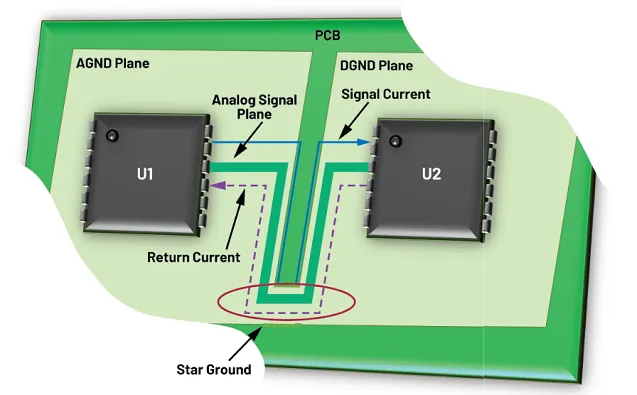
Many modern audio amplifiers include both analog and digital components, such as microcontrollers for control functions. Mixing these signals can lead to crosstalk, where digital noise interferes with sensitive analog audio signals. To prevent this, physically separate analog and digital sections on the PCB.
Use distinct ground planes for analog and digital circuits, connecting them at a single point (often called a star ground). This approach isolates noise from digital switching and keeps the audio signal pure. If space is tight, consider a multi-layer PCB design to dedicate separate layers for each type of signal.
Impedance Matching: The Key to Efficient Signal Transfer
Impedance matching ensures that the source, trace, and load in a circuit have compatible impedance values, allowing maximum power transfer and minimal signal reflection. In audio amplifier PCBs, improper impedance matching can cause signal loss or distortion, especially with high-frequency signals.
Why Impedance Matching Matters
In audio systems, speakers often have an impedance of 4 to 8 ohms, while amplifier outputs and traces may differ. Without matching, energy is reflected back, creating standing waves that distort the audio. For high-frequency signals (like those above 10 kHz), this effect becomes even more pronounced.
How to Achieve Impedance Matching
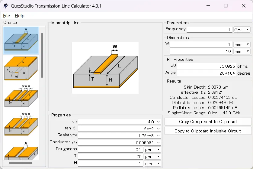
To match impedance, calculate the characteristic impedance of your PCB traces and ensure they align with the components. Use the formula for characteristic impedance in a microstrip trace:
Z0 = (87 / √(Er + 1.41)) * ln(5.98 * h / (0.8 * w + t))
Where:
- Z0 is the characteristic impedance (in ohms),
- Er is the dielectric constant of the PCB material (typically 4.5 for FR-4),
- h is the height of the dielectric layer (in mils),
- w is the trace width (in mils),
- t is the trace thickness (in mils).
For a typical audio amplifier PCB, aim for a trace impedance close to the load (e.g., 8 ohms for a speaker). Adjust trace width and layer spacing during design to achieve this. If calculations seem complex, many PCB design tools include impedance calculators to simplify the process.
Trace Width: Balancing Current and Signal Integrity
Trace width plays a dual role in audio amplifier PCB design. It affects both the current-carrying capacity and the impedance of the signal path. Choosing the right trace width is essential for maintaining signal integrity and preventing overheating.
Determining the Right Trace Width
For audio signals, traces don’t usually carry high currents (unlike power supply lines). A trace width of 10-20 mils (0.010-0.020 inches) is often sufficient for signal paths. However, for power delivery to the amplifier, wider traces are needed to handle higher currents without voltage drops or heat buildup.
Use a trace width calculator to determine the appropriate size based on current and temperature rise. For instance, a 1-amp current on a standard 1 oz copper PCB might require a 50-mil trace width to keep temperature rise below 10°C.
Impact on High-Frequency Signals
For high-frequency signals, narrower traces can increase impedance, leading to signal loss. Balance this by keeping traces short and using the impedance formula mentioned earlier to fine-tune width. Consistency in trace width also prevents sudden impedance changes, which can cause reflections.
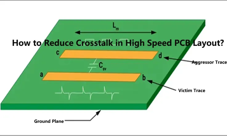
Minimizing Crosstalk for Cleaner Audio
Crosstalk occurs when signals from one trace interfere with another due to electromagnetic coupling. In audio amplifier PCBs, crosstalk can mix unwanted noise or other channels into the audio output, degrading sound quality.
Strategies to Reduce Crosstalk
Here are proven techniques to minimize crosstalk in your PCB design:
- Increase Trace Spacing: Keep parallel signal traces at least 3 times the trace width apart (known as the 3W rule). For a 10-mil trace, maintain a 30-mil gap to reduce coupling.
- Use Ground Planes: Place a solid ground plane beneath signal traces to shield them from interference. This acts as a barrier, absorbing stray electromagnetic fields.
- Route Signals on Different Layers: If space is limited, route sensitive audio signals on separate layers of a multi-layer PCB, with a ground plane between them.
- Avoid Parallel Routing: Route traces perpendicular to each other whenever possible to minimize the length over which they can couple.
By applying these methods, you can significantly reduce crosstalk and ensure each audio channel remains isolated for clear sound reproduction.
Handling High-Frequency Signals in Audio Amplifiers
While audio signals typically range from 20 Hz to 20 kHz, some modern designs involve high-frequency signals for switching power supplies or digital processing. These signals are more prone to issues like signal reflection, EMI, and crosstalk.
Challenges with High-Frequency Signals
At frequencies above 100 kHz, traces behave more like transmission lines, where impedance mismatches cause reflections. Additionally, high-frequency noise from switching regulators can couple into audio traces, creating audible interference.
Best Practices for High-Frequency Routing
- Controlled Impedance Traces: Design traces with specific impedance (e.g., 50 ohms) for high-frequency signals using the earlier formula. This prevents reflections and signal loss.
- Use Decoupling Capacitors: Place 0.1 μF capacitors near power pins of high-frequency components to filter noise and stabilize voltage.
- Minimize Loop Areas: Keep power and ground traces close together to reduce the loop area, which minimizes EMI radiation.
- Isolate High-Frequency Components: Physically separate high-frequency circuits (like switching power supplies) from audio signal paths to avoid interference.
By carefully managing high-frequency signals, you can prevent them from degrading the audio performance of your amplifier.
Grounding Techniques for Noise-Free Audio
Grounding is one of the most critical aspects of audio amplifier PCB design. A poorly designed ground can introduce ground loops, leading to a low-frequency hum in the audio output.
Star Grounding for Minimal Noise
Implement a star grounding scheme, where all ground connections meet at a single point. This prevents current from different parts of the circuit from flowing through shared ground paths, which can induce noise. For example, connect the grounds of the input stage, output stage, and power supply to one central point near the power input.
Ground Planes for Shielding
In multi-layer PCBs, dedicate an entire layer to a ground plane. This provides a low-impedance path for return currents and shields sensitive traces from noise. Ensure the ground plane is unbroken under critical audio signal paths to maximize its effectiveness.
Final Tips for Designing Audio Amplifier PCBs
Designing an audio amplifier PCB with excellent signal integrity requires attention to detail and adherence to best practices. Here are some final tips to keep in mind:
- Simulate your design using PCB design software to identify potential issues like crosstalk or impedance mismatches before manufacturing.
- Test prototypes with real audio signals to detect any noise or distortion that simulations might miss.
- Choose high-quality PCB materials with consistent dielectric properties to maintain impedance control.
- Keep power supply traces wide and short to avoid voltage drops that could affect amplifier performance.
Conclusion: Achieving Crystal-Clear Sound with Proper Routing
Signal integrity is the backbone of any high-performing audio amplifier PCB. By mastering audio amplifier PCB signal routing techniques—such as impedance matching, proper trace width selection, minimizing crosstalk, and managing high-frequency signals—you can create designs that deliver exceptional sound quality. Thoughtful layout, grounding, and separation of signal types are your tools to eliminate noise and distortion.
Whether you're building a simple stereo amplifier or a complex audio system, these principles will guide you toward success. Start applying these routing techniques in your next project, and experience the difference of crystal-clear sound firsthand.


