ALLPCB


Introduction
Historically, digital design was relatively simple. Designers could develop circuits operating up to about 30 MHz without accounting for transmission-line effects, because at lower frequencies the signals remained within acceptable digital margins and the system functioned correctly. As system performance increased, designers began to face additional challenges - higher frequencies mean that designers must consider not only digital behavior but also analog effects within the system.
Transmission Lines and High-Speed I/O
Many of the most significant design challenges relate to I/O signals, where transmission-line effects can substantially affect transmitted data. At low speeds, frequency response has little impact on signals unless the transmission medium is particularly long. As speed increases, high-frequency effects dominate, and even very short traces can exhibit ringing, crosstalk, reflections, and ground bounce, which degrade signal fidelity and compromise signal integrity. In practice, these issues can be mitigated by sound design techniques and adherence to simple layout rules.
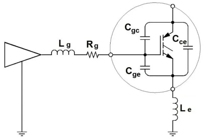
A transmission line is a connection that carries signals between a driver and a receiver. Traditionally, transmission lines referred to long-distance telecom cables. With high-speed digital signals, however, even short passive printed circuit board (PCB) traces behave as transmission lines and exhibit associated effects.
Distributed Properties and Characteristic Impedance
At low frequencies, a wire or PCB trace may approximate an ideal circuit without resistance, capacitance, or inductance. At higher frequencies, AC circuit behavior dominates, and impedance, inductance, and capacitance are distributed along the conductor. A circuit model can be used to determine the trace characteristic impedance. This characteristic impedance is critical because any impedance mismatch along the path will degrade signal quality.
Impedance Mismatch and Reflections
Impedance mismatch occurs when the source output impedance (Zs), the line impedance (Zo), and the receiver or load impedance (Zl) are not equal. The result is that the transmitted signal is not fully absorbed by the receiver and excess energy is reflected back toward the transmitter. This process repeats until the energy is dissipated. At high data rates, these reflections can produce overshoot, undershoot, ringing, and stepped waveforms that can cause errors.
Impedance mismatch is resolved when the transceiver buffers are matched to the transmission medium. For PCBs, this is achieved by selecting appropriate board materials and using proper termination schemes.
Termination Methods
Various termination methods can be used depending on the application. Methods may include simple parallel termination for certain devices, or more complex RC termination networks where an RC network provides a low-pass filter to attenuate low-frequency effects while allowing high-frequency components to pass. While external components often improve signal integrity, they consume PCB area and may require short stub traces that can introduce additional issues.
Some FPGA families include on-chip programmable termination to reduce the need for external components. On-chip termination techniques are available for both single-ended and differential I/O, and high-speed transceiver modules often include programmable termination schemes that support multiple high-speed I/O standards. In addition to termination, good PCB design practices are essential to address signal integrity challenges.
Loss Mechanisms in Transmission Media
High-frequency signals experience losses on transmission lines that impair the receiver's ability to interpret information. Common causes of loss in transmission media include:
| Cause | Description |
|---|---|
| Dielectric absorption | High-frequency signals activate molecular processes in the dielectric, causing it to absorb signal energy and reduce signal amplitude. Dielectric absorption depends on the PCB material and can be improved by careful material selection. |
| Skin effect | AC and high-frequency currents tend to flow near the conductor surface, increasing the effective inductive reactance at high frequencies and reducing the effective conductive area. The resulting rise in resistance increases signal attenuation. Increasing trace width can reduce skin-effect losses, but this is not always practical. |
Crosstalk
Whenever a signal is driven along a conductor, a magnetic field forms around it. If two conductors run adjacent to each other, their magnetic fields can interact and cause energy to couple between signals, known as crosstalk. The main coupling mechanisms that cause crosstalk are:
| Coupling | Description |
|---|---|
| Mutual inductance | Inductive coupling from a driven trace induces currents in a nearby quiet trace via the magnetic field. Mutual inductance produces a positive-going waveform at the near end (closest to the transmitter) of the victim trace and a negative-going waveform at the far end, resulting in near-end and far-end crosstalk. |
| Mutual capacitance | Capacitive coupling occurs between two electric fields, injecting current into the victim trace proportional to the rate of change of voltage in the aggressor. Mutual capacitance typically produces positive-going waveforms at both ends of the victim trace. |
PCB Techniques to Reduce Crosstalk
Careful PCB design can significantly reduce crosstalk. Typical mitigation steps include:
- Maximize spacing between signal traces where routing constraints allow
- Route traces close to a ground plane so the trace is tightly coupled to the ground plane, which helps decouple it from adjacent signals
- Use differential routing techniques whenever possible, especially for critical signal paths
- Place signals on different layers and route orthogonally where obvious coupling exists
- Minimize parallel run length between signals; use short parallel segments and avoid long coupling sections between nets
Ground Bounce and Simultaneous Switching Outputs (SSO)
As digital circuit speeds increase, output transition times shorten. Faster switching produces larger transient currents as load capacitances are discharged. If multiple outputs switch simultaneously from logic high to logic low, charge stored in I/O load capacitances returns to the device. The resulting surge current travels through internal inductances to the PCB ground, causing voltage fluctuations. This produces a voltage difference between the device and the board ground, briefly creating a low-voltage condition on I/O pins above ground. This phenomenon is known as ground bounce. Ground bounce can cause a driven low to be seen as a high by other devices on the board.
Ground bounce can be reduced by following PCB-based design rules such as those outlined in AN 315: High-Speed FPGA PCB Design Guidelines (PDF). High-speed device features such as pin slew-rate control allow designers to slow driver edges to reduce ground bounce. Devices also provide multiple power and ground pins so that high-speed I/O pins can be placed near ground pins to mitigate the effects of simultaneous switching outputs. Addressing high-speed design challenges requires careful analog design practices and careful PCB layout techniques. High-speed programmable logic devices often include features such as programmable slew-rate control and on-chip termination to support high-speed designs.