ALLPCB


1. EMI Sources
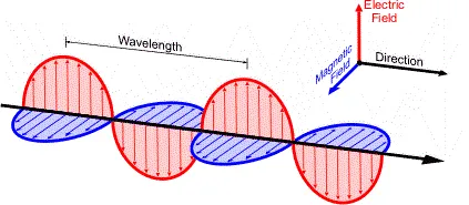
Two types of radiation sources cause EMI problems: alternating electric fields (high impedance) and alternating magnetic fields (low impedance). Non-isolated DC/DC converters have very low impedance nodes and loops (much lower than the 377Ω impedance of free space), so the primary radiation source in a buck converter topology is typically the magnetic field.
Magnetic field radiation is generated by high-frequency currents in small current loops. The high-frequency magnetic field produced by a current loop gradually transforms into an electromagnetic field at a distance of approximately 0.16λ from the loop. The resulting field strength can be approximated by:
Where f is the signal frequency in Hz, A is the area of the current loop in m², I is the current amplitude in the loop in A, and R is the distance from the loop to the measurement point in m.
For example, a 1 cm² current loop with a 1 mA current switching at 100 MHz will produce a field strength of 4.4 μV/m (12.9 dBμV) at a distance of 3 meters.
2. Buck Converter Current Loops
A buck converter has two main loops where current changes abruptly:
When the high-side MOSFET Q1 is on, current flows from the power source through Q1 and L1 to the output capacitor and load, then returns to the power source input through the ground path. During this phase, the AC component of the current flows through the input and output capacitors.
When Q1 turns off, the inductor current continues to flow in the same direction, and the synchronous rectifier MOSFET Q2 turns on. The current now flows through Q2, L1, and the output capacitor, returning to Q2 through ground. This path is shown in blue in Figure 2, labeled I2.
Both currents, I1 and I2, are discontinuous, meaning they have steep rising and falling edges during switching. These edges have very short rise and fall times, resulting in a high rate of current change (dI/dt) and containing many high-frequency components.
In the loops described above, I1 and I2 share the path from the switch node → inductor → output capacitor → ground → Q2 source. When combined, I1 and I2 form a relatively smooth, continuous sawtooth waveform. Since this combined current lacks sharp edges with high dI/dt, it contains fewer high-frequency components.
From an EMI perspective, the shaded area A1 in Figure 3 represents the loop with high dI/dt. This loop generates the most high-frequency components and is the most critical part to consider in the EMI design of a buck converter. The current change rate (dI/dt) in area A2 is lower than in A1, thus generating less high-frequency noise.
When designing the PCB layout for a buck converter, the area of loop A1 should be made as small as possible. Refer to section 6 for practical PCB layout guidelines.
3. Input and Output Filtering
Ideally, input and output capacitors present a very low impedance to the buck converter's switching currents. In practice, however, capacitors have ESR (Equivalent Series Resistance) and ESL (Equivalent Series Inductance), which increase their impedance and cause additional high-frequency voltage drops. This voltage drop creates corresponding current variations on the power supply lines and load connection circuits, as shown below.
Due to the discontinuous nature of the buck converter's input current and the typically long power supply lines, the radiation from the input loop A3 can be significant. This can lead to excessive conducted emissions in the 150 kHz to 30 MHz band, causing failures in EMC compliance testing.
To reduce the voltage drop across the input capacitor CIN, place multiple low-ESR MLCCs of different sizes close to the buck IC. For example, a combination of two 10μF capacitors in a 1206 package and 22nF to 100nF capacitors in 0603 or 0402 packages can be used. To reduce input loop noise, adding an extra LC filter on the input line is highly recommended. When using a pure inductor for L2, it's necessary to add an electrolytic capacitor C3 to suppress potential ringing on the power input and ensure stability.
For output filtering, also use multiple MLCCs of different sizes for the output capacitor, Cout. Small 0603 or 0402 capacitors (22nF to 100nF) can effectively block high-frequency noise from the switch node that couples to the output through the inductor L1's parasitic capacitance. Adding a high-frequency ferrite bead can prevent the output loop from acting as an effective loop antenna, but be aware that this can degrade the converter's load transient response and load regulation. If the application has strict requirements in these areas, avoid the bead and instead place the converter as close to the load as possible, optimizing the copper traces to minimize loop area.
4. Slowing the Converter's Switching Speed
If optimizing the PCB layout and filtering is still not enough to bring a buck converter's radiation below the required level, the next step is to slow down the converter's switching speed. This can be very helpful in reducing its radiation levels.
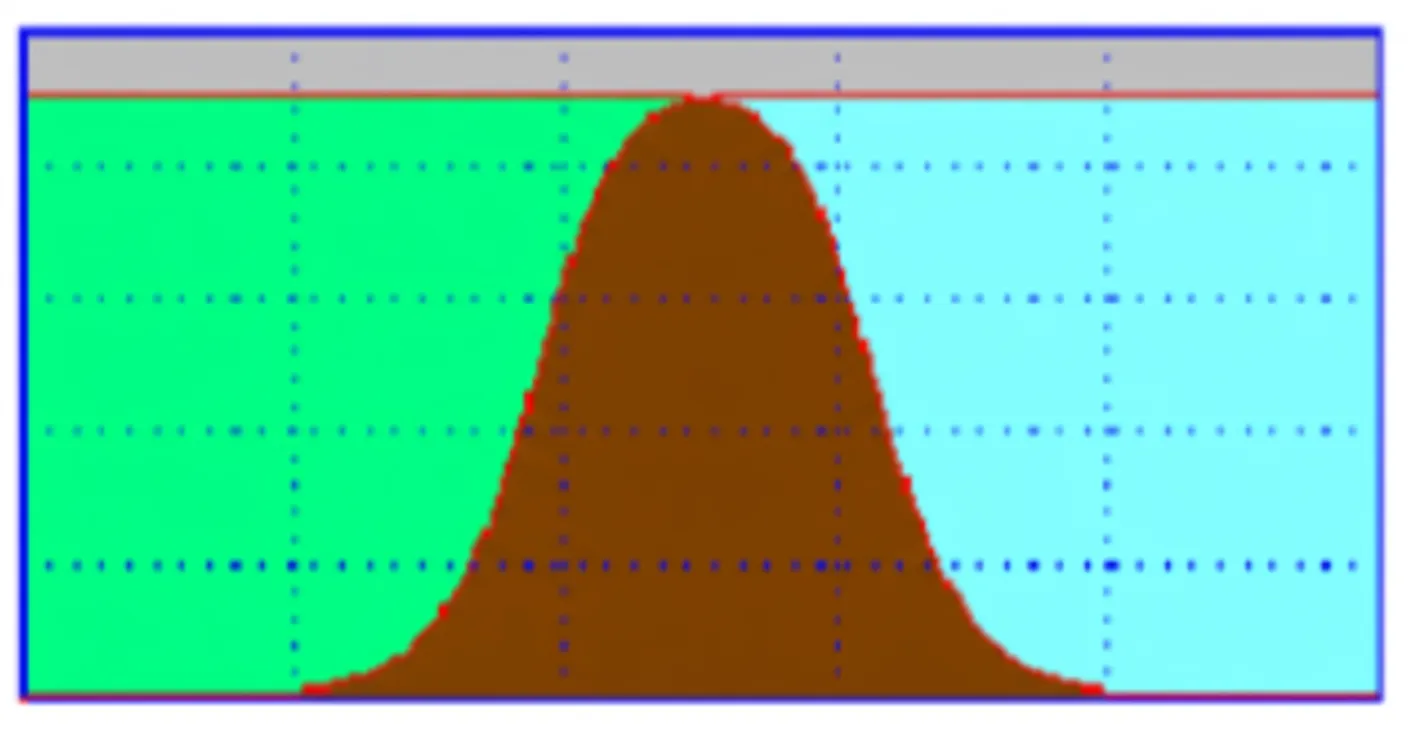
To understand the extent of this improvement, we need to examine the high-frequency components of a discontinuous current pulse. The left side of Figure 6 shows a simplified trapezoidal current waveform with period TPERIOD, pulse width TW, and rise/fall time TRISE. In the frequency domain, this signal contains a fundamental frequency and many higher-order harmonics. Fourier analysis shows the relationship between the amplitude of these high-frequency components and the pulse width and rise/fall time, as illustrated on the right side of the figure below.
EMI radiation problems often occur in the 50 MHz to 300 MHz frequency range. By increasing the rise and fall times, the corner frequency fR is shifted to a lower frequency, and the amplitude of higher frequency signals decreases rapidly at a rate of 40 dB/decade, thereby improving radiation performance. The improvement at lower frequencies from slower rise and fall times is limited.
Adding a Series Resistor to the Bootstrap Circuit
The rise time of the switching waveform depends on the turn-on speed of the high-side MOSFET, Q1. Q1 is driven by a floating driver powered by the bootstrap capacitor, Cboot. In integrated buck converters, Cboot is supplied by an internal regulator, typically providing 4V to 5V. See the left side of the figure below.
Slowing the turn-on speed of the high-side MOSFET increases the rise time of the buck converter's switching waveform and current pulse. This can be achieved by adding a series resistor, Rboot, to Cboot, as shown in the figure above. The value of Rboot depends on the size of the high-side MOSFET; for most applications, 5-10Ω is sufficient. For smaller MOSFETs with higher RDS(on), a larger Rboot value is permissible. In high duty-cycle applications, too large an Rboot value may cause Cboot to undercharge and could even lead to instability in the current sense circuit. Additionally, a slower MOSFET turn-on speed increases switching losses, reducing efficiency.
In designs with external MOSFETs, a resistor can be placed in series with the high-side MOSFET's gate, which will increase both its turn-on and turn-off times.
When the high-side MOSFET Q1 turns off, the inductor current charges Q1's parasitic output capacitance while discharging Q2's parasitic output capacitance until the switch node potential drops below ground and Q2's body diode conducts. Therefore, the fall time is primarily determined by the peak inductor current and the total parasitic capacitance at the switch node.
5. Managing Parasitic Ringing
The figure below shows the parasitic components in a typical buck converter IC.
These parasitic capacitances are formed by the MOSFET's Coss and the capacitance to the substrate. There is also parasitic inductance in the bond wires connecting the IC pins to the silicon die. These parasitics, along with the parasitic inductance from the PCB layout and the ESL of the input filter capacitor, cause high-frequency ringing on the switching waveform. When MOSFET Q1 turns on, ringing on the switch node's rising edge is mainly caused by Q2's Coss and the total parasitic inductance in the switching path (LpVIN + LpGND + LpLAYOUT + ESLCIN). When MOSFET Q1 turns off, ringing on the falling edge is mainly caused by Q1's Coss and the parasitic inductance from the low-side MOSFET's source to ground (LpGND).
The figure above shows a switch node waveform with fast rise and fall times, both exhibiting ringing. Since the energy stored in a parasitic inductor is ½I²Lp, the amplitude of the ringing increases with load current. The frequency of this ringing is typically in the 200-400 MHz range and can cause high-frequency EMI. Excessive ringing usually indicates large parasitic inductance, suggesting a need to review and correct the PCB layout for issues like large loops or overly narrow VIN and/or ground traces. Component packaging also affects ringing; wire-bonded packages have more parasitic inductance than flip-chip packages because bond wires have more inductance than solder bumps, resulting in worse performance.
RC Snubber Circuit
Adding an RC snubber circuit can effectively dampen ringing, but it increases switching losses.
The RC snubber should be placed very close to the switch node and power ground. In a buck converter with external MOSFETs, the RC snubber should be placed directly across the drain and source of the low-side MOSFET. The figure below illustrates the placement of an RC snubber.
The snubber resistor Rs provides sufficient damping for the parasitic LC resonant circuit. Its value depends on the desired damping strength and the parasitic L and C parameters, and can be determined by the following formula:
Where ξ is the damping factor, typically chosen between 0.5 (light damping) and 1 (critical damping). The parasitic parameters Lp and Cp are usually unknown but can be measured as follows:
- Measure the original ringing frequency, fRING, on the rising edge of the signal.
- Add a small capacitor between the switch node and ground. This will lower the ringing frequency. Continue increasing the capacitance until the ringing frequency is 50% of the original frequency.
- A 50% reduction in ringing frequency means the total resonant capacitance is now 4 times the original capacitance. Therefore, the original parasitic capacitance Cp is 1/3 of the added capacitance.
The parasitic inductance Lp can then be calculated:
The series capacitor Cs in the RC snubber needs to be large enough for the damping resistor to provide stable damping during resonance. If this capacitor is too large, its charging and discharging in each switching cycle will cause excessive power dissipation. Therefore, Cs is typically chosen to be 3 to 4 times the value of the parasitic capacitance Cp.
In addition to damping resonance, an RC snubber circuit can also slightly slow down the rise and fall speeds of the switching waveform. Furthermore, the charging and discharging of the snubber capacitor creates additional current spikes during switching transitions, which can cause new EMI problems at lower frequencies.
When using an RC snubber, always check the total power loss of the circuit. The converter's efficiency will inevitably decrease, especially at high switching frequencies and high input voltages.
6. Key Points for Buck Converter PCB Layout
The key to a good buck converter PCB layout is to plan the placement of critical components from the beginning.
- In noise-sensitive applications, it's best to choose small, low-inductance flip-chip packages.
- Identify the VIN and GND nodes of the switching loop and place input capacitors of various sizes as close as possible to these nodes, with the smallest capacitor being the closest. Since this "hot loop" carries a high dI/dt, it must be kept as small as possible.
- Place the ground of the output capacitors in an area that does not overlap with the input capacitor's switching path to prevent high-frequency noise from coupling into the output voltage.
- The converter's small-signal section should be separated from the high-power switching section. Its ground should be connected to a clean, quiet area, and never allow input current signals or output ripple current to flow into it.
- When using a ground plane, strive to keep the ground layer under the input switching loop solid and uninterrupted. Any cuts in this area reduce the effectiveness of the ground plane; even signal vias passing through the ground plane increase its impedance.
- Vias can be used to connect decoupling capacitors and the IC's ground to the ground plane, which helps shorten the loop. However, remember that a via has an inductance of about 0.1-0.5 nH, depending on its thickness and length, which adds to the total loop inductance. For low-impedance connections, use multiple vias.
- Be aware that using the ground plane as a current return path will introduce significant noise into it. One solution is to create a local ground island and connect it to the main ground at a single, quiet point.
- The shielding effect of a ground plane is significantly enhanced when it is very close to the radiating loop. Therefore, when designing a multilayer PCB, place a solid ground plane on the second layer, directly beneath the top layer that carries high currents.
- Unshielded inductors generate a large amount of magnetic flux leakage, which can couple into other loops and filter components. In noise-sensitive applications, use semi-shielded or fully shielded inductors and keep sensitive circuits and loops away from the inductor.
7. Simple DIY EMI Probes
Measuring EMI compliance usually means taking your product prototype to an EMC lab, which typically has a 3-meter anechoic chamber and specialized antennas and receivers. While this provides final system-level results, it's not always easy to find the root cause of a specific radiation problem in such an environment.
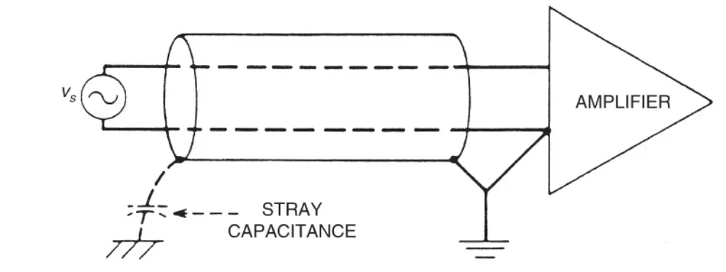
It is possible to perform some basic EMI tests on a prototype in a lab setting, even on individual modules of the system. Such tests are typically conducted in the near-field (measurement distance < 0.16λ). To test the radiation of current loops, you need a small loop antenna to measure the high-frequency magnetic field. You can make a small, shielded loop antenna yourself using a piece of 50Ω coaxial cable, as shown in the diagram below.
This loop antenna can be connected to a spectrum analyzer. By moving it over the PCB, you can identify areas with strong high-frequency magnetic fields. You can also connect it to an oscilloscope (using a 50Ω termination), which will display the switching noise level in that area. By keeping the relative position and distance between the antenna loop and the board constant while making changes to the circuit or PCB loops, you can see whether the noise level increases or decreases.
Since radiation from power cables has a significant impact on EMI levels, you can also measure the high-frequency currents on these cables. Not all current probes have enough bandwidth to highlight EMI problems. This can be addressed by creating a high-frequency current transformer by winding several turns of wire through an EMI ferrite core. The method is similar to making the loop antenna, but requires passing the loop through the core three times. See the figure below.
Now you can measure the high-frequency current in a cable by passing it through the core. The output of the current transformer can be connected to a spectrum analyzer or oscilloscope (using a 50Ω input).
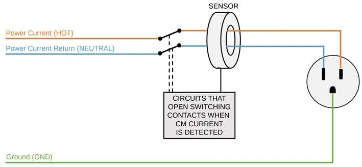
To isolate the test tool from the device under test, it's best to add a common-mode choke to the cable. This can be done by passing the cable leading to the analysis equipment through a clamp-on EMI ferrite core several times.
Passing both the positive and negative power wires through the core in the same direction measures the common-mode current. Reversing the direction of one of the wires measures the differential-mode current. See the figure above.
Another handheld tool is a current probe, which is a miniaturized current transformer with an open core. See the figure below. This tool can be used to measure high-frequency currents on PCB traces or component pins.
A current probe allows you to see how changing high-frequency currents flow on the board and through components. It can even show how current flows on a copper trace: you will find that high-frequency current always takes the shortest path. In fact, even eddy currents in the ground plane can be measured.
8. Conclusion
Solving EMI problems can be a complex task, especially when dealing with a complete system without knowing the source of the radiation. However, with a foundational knowledge of high-frequency signals and current loops in switching converters, an understanding of how components and PCB layouts behave at high frequencies, and the use of simple DIY tools, it is possible to find radiation sources and implement low-cost solutions to easily resolve EMI issues.
The primary source of radiation in a buck converter is its input switching loop, which should be the main focus of your analysis. The choice of component packaging for the switching converter can play a crucial role in achieving an optimal layout for the lowest possible EMI.
Slowing down the converter's switching speed can help reduce EMI, but it is often not the optimal solution. Shielding with a ground plane is very effective; ground planes should be as large and solid as possible and placed as close as possible to the radiating loops. Filtering the input and output lines is very effective for reducing conducted emission levels.