 ALLPCB


Grounding is a cornerstone of effective Printed Circuit Board (PCB) design. If you're looking to reduce noise and ensure reliable connections in your circuits, proper PCB grounding techniques are essential. In this comprehensive guide, we'll explore the best practices for PCB grounding, focusing on noise reduction, creating reliable connections, using bypass capacitors, and optimizing power supply design. Whether you're a beginner or an experienced engineer, this blog will provide actionable tips to improve your PCB performance.
Why PCB Grounding Matters for Noise Reduction and Reliability
Grounding in PCB design serves as the foundation for stable electrical performance. A well-designed ground system minimizes noise, prevents interference, and ensures that signals and power are delivered reliably across the board. Poor grounding can lead to issues like electromagnetic interference (EMI), ground loops, and signal distortion, which can degrade the performance of your device or even cause it to fail.
By implementing effective grounding techniques, you can achieve noise reduction, maintain signal integrity, and create reliable connections between components. Let’s dive into the key principles and methods to achieve this.
Understanding the Basics of PCB Grounding
Before we explore advanced techniques, let's cover the fundamentals of PCB grounding. Grounding refers to connecting parts of a circuit to a common reference point, usually a ground plane or a ground trace, to provide a stable return path for current. This helps to keep voltage levels consistent and reduces unwanted noise.
In a PCB, the ground serves multiple purposes:
- Noise Reduction: It prevents interference by providing a low-impedance path for stray currents.
- Signal Integrity: It maintains stable reference voltages for signals, especially in high-speed designs.
- Safety: It protects users and components by directing fault currents away from sensitive areas.
Without proper grounding, you might encounter issues like crosstalk between traces or erratic behavior in your circuit. Now, let’s look at specific techniques to optimize grounding for noise reduction and reliable connections.
Key PCB Grounding Techniques for Noise Reduction
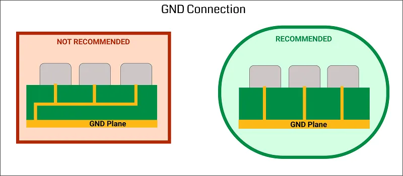
1. Use a Dedicated Ground Plane
One of the most effective ways to reduce noise in a PCB is by using a dedicated ground plane. A ground plane is a large, continuous layer of copper on the PCB that acts as a common ground reference for all components. It provides a low-impedance path for return currents, minimizing noise and interference.
For example, in a 4-layer PCB, one layer is often dedicated entirely to grounding. This setup can reduce EMI by up to 20 dB compared to designs with only ground traces. Ensure the ground plane is unbroken as much as possible—avoid splitting it with traces or vias unless absolutely necessary, as splits can create high-impedance paths and increase noise.
2. Minimize Ground Loops
Ground loops occur when there are multiple paths for ground currents to flow, creating differences in potential that can introduce noise. To avoid ground loops, ensure all components connect to a single ground point or plane. This is especially important in mixed-signal designs where analog and digital signals coexist.
For instance, if you’re designing a board with both analog sensors and digital microcontrollers, separate the analog and digital ground planes but connect them at a single point near the power supply. This prevents digital switching noise (which can reach frequencies of 100 MHz or more) from interfering with sensitive analog signals.
3. Shorten Return Paths
Return paths are the routes that currents take back to their source. Long return paths increase impedance and can lead to noise and signal delays. To minimize this, place components close to their ground connections and route signal traces over the ground plane to ensure the return path is as short as possible.
In high-speed designs, such as those operating at 1 GHz or above, a long return path can introduce signal delays of several nanoseconds, leading to timing errors. Keeping return paths short ensures reliable connections and better noise reduction.
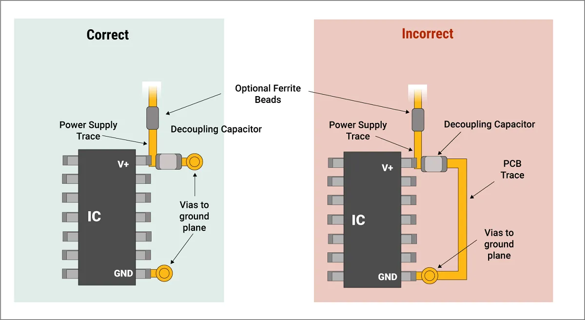
Using Bypass Capacitors for Noise Reduction
Bypass capacitors, also known as decoupling capacitors, play a critical role in PCB grounding and noise reduction. These capacitors are placed between the power supply and ground near active components like ICs to filter out high-frequency noise and stabilize voltage levels.
Here’s how to use bypass capacitors effectively:
- Placement: Position bypass capacitors as close as possible to the power pins of ICs. A distance of less than 0.1 inches (2.54 mm) is ideal to minimize inductance.
- Value Selection: Use a combination of capacitor values, such as 0.1 μF and 1 μF, to filter a wide range of frequencies. For example, a 0.1 μF capacitor can handle noise up to 100 MHz, while a larger 10 μF capacitor addresses lower-frequency fluctuations.
- Ground Connection: Connect the capacitor directly to the ground plane with a short via to reduce parasitic inductance, which can otherwise negate the capacitor’s effectiveness.
By using bypass capacitors strategically, you can achieve significant noise reduction, ensuring that your power supply remains stable even during rapid switching events.
Optimizing Power Supply Design for Reliable Connections
The power supply is another critical area where grounding techniques can improve reliability and reduce noise. A poorly designed power supply layout can introduce ripple and interference, affecting the entire circuit. Here are some best practices for integrating grounding with power supply design:
1. Separate Power and Ground Planes
In multilayer PCBs, dedicate separate layers for power and ground planes. Place these layers adjacent to each other to create a natural capacitance effect, which helps filter out noise. For example, in a 6-layer board, you might have the ground plane on layer 2 and the power plane on layer 3, keeping them close for better coupling.
2. Use Star Grounding for Power Distribution
Star grounding involves connecting all ground points to a central node, usually near the power supply input. This method prevents ground loops and ensures that noise from one part of the circuit doesn’t affect others. It’s particularly useful in designs with multiple power domains, such as a board with 3.3V and 5V sections.
3. Route Power Traces Carefully
When routing power traces, keep them short and wide to reduce resistance and inductance. A trace width of 20 mils (0.5 mm) or more is recommended for power lines carrying 1A of current to minimize voltage drops. Also, avoid running power traces over splits in the ground plane, as this can disrupt return paths and introduce noise.
By focusing on these power supply grounding techniques, you ensure reliable connections and a stable voltage supply, which are crucial for the overall performance of your PCB.
Related Reading: Understanding AGND and DGND Grounding Practices
Grounding for Mixed-Signal Designs
Mixed-signal PCBs, which combine analog and digital components, require special attention to grounding. Digital circuits often generate high-frequency noise that can interfere with sensitive analog signals. To address this, follow these guidelines:
- Separate Analog and Digital Grounds: Use separate ground planes for analog and digital sections to isolate noise. Connect these planes at a single point, ideally near the power supply or ADC (analog-to-digital converter), to avoid ground loops.
- Route Signals Carefully: Keep digital traces away from analog components. For example, if a digital clock signal operates at 50 MHz, its harmonics can couple into nearby analog traces, causing errors in measurements.
- Use Shielding: If separation isn’t possible, consider adding guard traces or shielding around sensitive analog areas, connecting them to the analog ground.
These steps ensure that noise from digital components doesn’t compromise the accuracy of analog signals, maintaining reliable connections across the board.
Related Reading: Power Integrity in Mixed Signal PCBs: Minimizing Noise and Ensuring Stability
Common Grounding Mistakes to Avoid
Even with the best intentions, grounding mistakes can undermine your PCB design. Here are some common pitfalls and how to avoid them:
- Splitting Ground Planes Unnecessarily: Splitting a ground plane without a clear reason can create high-impedance return paths, increasing noise. Only split planes when separating analog and digital grounds, and connect them at a single point.
- Ignoring Via Placement: Vias connect components to the ground plane, but placing them far from components increases inductance. Always use multiple vias for high-current paths to reduce impedance.
- Neglecting Bypass Capacitors: Failing to use or improperly placing bypass capacitors can lead to power supply noise. Always include them near IC power pins.
By being aware of these mistakes, you can design PCBs with better noise reduction and more reliable connections.
Advanced Tips for High-Speed PCB Grounding
For high-speed designs, such as those involving USB, HDMI, or RF signals, grounding becomes even more critical. Here are some advanced techniques:
- Control Impedance: Ensure that the ground plane supports controlled impedance for high-speed traces. A typical 50-ohm impedance for RF signals requires a specific trace width and ground plane proximity, often calculated using PCB design software.
- Avoid Ground Plane Gaps: Gaps under high-speed traces can cause signal reflections. Keep the ground plane continuous beneath these traces.
- Use Stitching Vias: In multilayer boards, use stitching vias to connect ground planes across layers, reducing impedance and noise. Space vias at intervals of about 1/8th of the wavelength of the highest signal frequency (e.g., every 3.75 mm for a 10 GHz signal).
These advanced grounding techniques ensure that high-speed signals maintain their integrity, minimizing noise and ensuring reliable connections.
Conclusion: Building Better PCBs with Proper Grounding
Effective PCB grounding is the key to minimizing noise and ensuring reliable connections in your designs. By using a dedicated ground plane, minimizing ground loops, incorporating bypass capacitors, and optimizing power supply layouts, you can significantly improve the performance of your circuits. Whether you're working on a simple prototype or a complex high-speed board, these grounding techniques will help you achieve noise reduction and maintain signal integrity.
Remember to tailor your grounding approach to the specific needs of your design, whether it’s a mixed-signal board or a high-frequency application. With careful planning and attention to detail, you can create PCBs that perform reliably under any conditions.
Start applying these PCB grounding techniques in your next project to see the difference in noise reduction and connection reliability. Your designs will thank you for it!


