ALLPCB


Are you looking to improve your PCB design for manufacturing? This guide dives deep into key areas like material selection, design optimization, and troubleshooting tips to help you create high-quality, cost-effective printed circuit boards (PCBs). Whether you're a beginner or a seasoned engineer, you'll find practical advice to streamline your design process and avoid common pitfalls. Let’s explore how to master PCB design for manufacturing with actionable strategies and insights.
Introduction to PCB Design for Manufacturing
Designing a PCB is more than just creating a functional circuit; it’s about ensuring that the board can be manufactured efficiently and reliably. PCB design for manufacturing (DFM) focuses on optimizing every aspect of the design to reduce costs, improve quality, and minimize errors during production. By considering factors like material selection, layout efficiency, and potential issues early in the design phase, you can save time and resources while delivering a superior product.
In this blog, we’ll break down the essentials of PCB design for manufacturing, covering material selection to ensure durability and performance, design optimization for smoother production, and troubleshooting techniques to address common challenges. Let’s get started with the foundation of any successful PCB: choosing the right materials.
Material Selection: Building a Strong Foundation for Your PCB
The materials you choose for your PCB play a critical role in its performance, reliability, and cost. Selecting the right substrate, copper thickness, and surface finish can make the difference between a board that lasts years and one that fails prematurely. Here’s what you need to know about material selection for manufacturing.
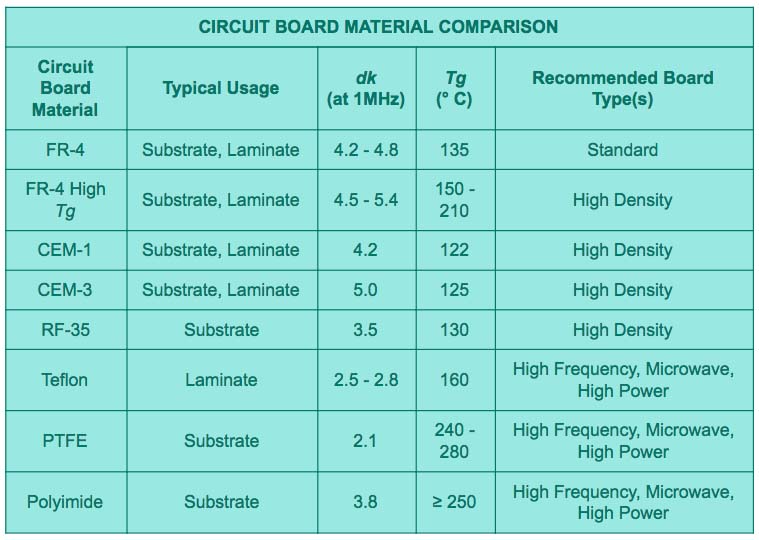
Choosing the Right Substrate Material
The substrate is the base material of your PCB, and it impacts thermal management, electrical performance, and mechanical strength. The most common substrate is FR-4, a fiberglass-epoxy laminate known for its balance of cost and performance. FR-4 typically has a dielectric constant of around 4.5 at 1 MHz, making it suitable for many standard applications. However, for high-frequency designs, materials like Rogers or Teflon with lower dielectric constants (around 2.2-3.5) may be necessary to minimize signal loss.
For high-temperature environments, consider high-Tg (glass transition temperature) substrates, which can withstand temperatures above 170°C without deforming. If your design operates in extreme conditions, ceramic or polyimide materials might be better choices despite their higher cost.
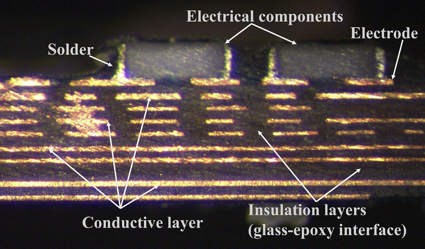
Copper Thickness and Weight
Copper thickness, measured in ounces per square foot (oz/ft2), determines how much current your PCB can handle. A standard 1 oz/ft2 copper layer can carry about 1.4 amps per 10 mils of trace width at 25°C. For power-heavy applications, you might need 2 oz/ft2 or thicker copper to handle higher currents without overheating. Keep in mind that thicker copper increases manufacturing costs, so balance performance needs with budget constraints.
Surface Finishes for Protection and Solderability
The surface finish protects the copper from oxidation and ensures good solderability. Common options include HASL (Hot Air Solder Leveling), which is cost-effective but less precise, and ENIG (Electroless Nickel Immersion Gold), which offers excellent flatness and durability for fine-pitch components. For high-reliability applications, ENIG is often preferred despite its higher cost, as it can reduce soldering defects by up to 30% compared to HASL in some studies.
Design Optimization: Streamlining Your PCB for Manufacturing
Design optimization is the heart of PCB design for manufacturing. A well-optimized design reduces production errors, cuts costs, and improves performance. Let’s explore key strategies to ensure your PCB layout is ready for the manufacturing process.
Follow Design for Manufacturability (DFM) Guidelines
DFM guidelines help ensure your design can be produced without issues. Start with proper trace width and spacing. For standard designs, a minimum trace width of 6 mils and spacing of 6 mils is often acceptable for most manufacturers. However, for high-density designs, you may need to go down to 3 mils, which requires advanced fabrication techniques and increases costs.
Keep components away from board edges—maintain at least a 0.1-inch (2.54 mm) clearance to avoid damage during depanelization. Also, ensure vias are not too close to pads or traces; a minimum annular ring of 5 mils around vias prevents drilling errors.
Optimize Component Placement
Place components logically to minimize trace lengths, especially for high-speed signals. For example, in a design with a microcontroller operating at 100 MHz, keeping critical signal traces under 1 inch can help avoid signal integrity issues due to delays or interference. Group similar components together, such as decoupling capacitors near power pins, to reduce noise. A 0.1 μF capacitor placed within 0.2 inches of a power pin can reduce voltage ripple by up to 50% in some circuits.
Manage Thermal Performance
Heat dissipation is a common challenge in PCB design. Use thermal vias under high-power components to transfer heat to a ground plane or heat sink. For a power IC dissipating 5 watts, placing 9-16 thermal vias (0.3 mm diameter each) can lower the junction temperature by 10-15°C. Additionally, consider wider copper planes for heat distribution— a 2 oz/ft2 copper layer can handle twice the thermal load of a 1 oz/ft2 layer.
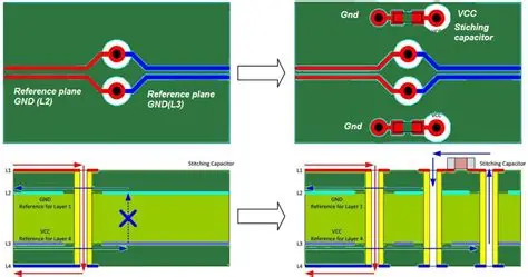
Signal Integrity and Impedance Control
For high-speed designs, signal integrity is critical. Maintain controlled impedance for traces carrying signals above 50 MHz. A 50-ohm impedance trace on FR-4 typically requires a width of 6 mils on a 1.6 mm board with a ground plane. Use simulation tools to verify impedance and avoid reflections that can degrade signal quality by up to 20% in high-speed applications.
Troubleshooting: Identifying and Fixing Common PCB Design Issues
Even with careful planning, issues can arise during PCB design or manufacturing. Knowing how to troubleshoot these problems can save you time and money. Below are some common challenges and solutions to keep your project on track.
Signal Noise and Crosstalk
Noise and crosstalk often occur in high-speed designs due to poor grounding or close trace spacing. If you notice erratic behavior in a circuit operating at 200 MHz, check for ground loops or insufficient decoupling. Adding a 0.01 μF capacitor in parallel with a 0.1 μF capacitor near noisy ICs can filter out high-frequency noise effectively. Also, increase spacing between high-speed traces to at least 3x the trace width to reduce crosstalk by up to 40%.
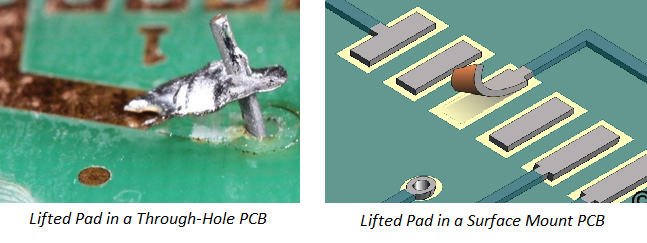
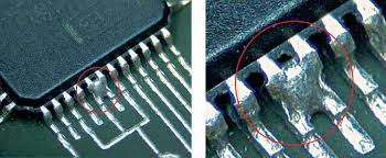
Soldering Defects
Soldering issues like cold joints or tombstoning can occur due to improper pad sizes or thermal imbalance. Ensure pad sizes match component footprints—a 0603 resistor typically needs pads of 1.0 mm x 0.6 mm for reliable soldering. For unbalanced designs, add copper balancing on both sides of the board to prevent uneven heating during reflow, which can reduce tombstoning by 25% in surface-mount assembly.
Manufacturing Errors
Manufacturing errors like misaligned layers or drill hits often stem from unclear design files or insufficient tolerances. Always provide clear Gerber files with a detailed fabrication drawing. Specify tolerances for critical dimensions—for instance, a ±0.1 mm tolerance on via placement can prevent alignment issues in multilayer boards. Double-check drill files to ensure via sizes match your design; a 0.3 mm via drilled at 0.4 mm can weaken connections by 15%.
Best Practices for Successful PCB Design for Manufacturing
Beyond the core areas of material selection, design optimization, and troubleshooting, adopting best practices can elevate your PCB design process. Here are some proven tips to ensure success.
Collaborate Early with Manufacturers
Engage with your manufacturing partner during the design phase. Share your design files early to get feedback on potential issues like stack-up configurations or material availability. Many manufacturers offer free DFM checks that can catch up to 70% of common design errors before production starts.
Use Design Software Tools
Leverage PCB design software with built-in DFM analysis to simulate and validate your layout. Tools that check for trace spacing, via placement, and impedance can reduce design iterations by 30%. Ensure your software exports standard file formats like Gerber and ODB++ for seamless communication with manufacturers.
Test and Iterate
Build prototypes to test your design under real-world conditions. For a power supply board delivering 5V at 2A, measure output ripple with an oscilloscope to ensure it stays below 50 mV. Use test results to refine your design, adjusting component values or layout as needed before full-scale production.
Conclusion: Master PCB Design for Manufacturing
Mastering PCB design for manufacturing requires attention to detail across material selection, design optimization, and troubleshooting. By choosing the right materials like FR-4 or high-Tg substrates, optimizing layouts for signal integrity and thermal management, and addressing issues like noise or soldering defects, you can create reliable, cost-effective PCBs that meet your project’s needs.
Start applying these strategies in your next design to streamline production and enhance performance. With careful planning and adherence to best practices, you’ll not only improve the quality of your boards but also reduce costs and time to market. Keep learning and refining your skills to stay ahead in the ever-evolving world of PCB design.