ALLPCB


Overview
This article summarizes the application requirements and implementation forms of packaged antennas in the context of heterogeneous integration, and provides examples using LTCC, HDI, and three types of interposer materials.
Contents
- Why heterogeneous integration is chosen
- Implementation of packaged antennas
Why heterogeneous integration is chosen
Millimeter-wave bands offer large bandwidth and abundant spectrum resources, meeting the high resolution and high data-rate requirements of communication systems. They are widely used in mobile communications, the Internet of Things, autonomous driving, and biomedical applications. At millimeter-wave frequencies, antennas and electronic devices scale down to millimeter dimensions, driving systems toward miniaturization, high efficiency, high integration, low power, and low cost.
In implementing high-performance millimeter-wave systems, a single silicon-based process or compound semiconductor processes (such as gallium arsenide or gallium nitride) cannot perfectly balance performance, cost, power, and integration requirements. Since Moore's observation in 1965 that integration density tends to double every 18-24 months under constant cost, silicon processes have steadily followed this scaling, achieving mature and highly integrated IC technologies down to recent nodes. Silicon processes remain the most mature option for high-density integration.
III-V compound semiconductors have wider bandgaps, higher breakdown fields, and better high-temperature tolerance, making them suitable for high-power and high-frequency devices due to their high electron mobility.
Implementation of packaged antennas
Antennas perform the essential conversion between electromagnetic waves and electrical signals in RF systems. The antenna-in-package (AiP) concept, introduced in 2006, advanced the development and adoption of packaged antenna technologies. In highly integrated millimeter-wave systems, packaged antennas balance compact size and performance, enabling close integration between chips and antenna elements. Figure 1 shows a representative packaged antenna design.
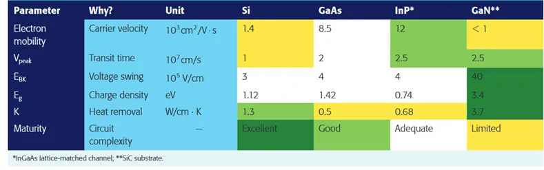
Figure 1. A packaged antenna structure
In 2009, Sun Mei and Professor Zhang Yueping applied grid antennas to packaged antenna design and used LTCC (low temperature co-fired ceramic) processing to realize a 60 GHz grid-array packaged antenna. The measured peak gain was 13.5 dBi and radiation efficiency exceeded 85% across the bandwidth, demonstrating LTCC's potential for packaged antennas.
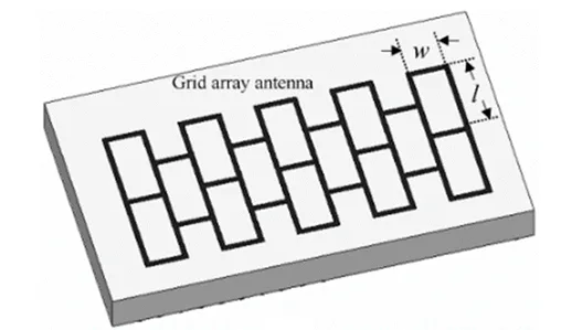
Figure 2. Grid array antenna
In 2017, a team at IBM investigated a packaged antenna for 5G Ka-band communications implemented using HDI (high-density interconnect). The HDI stack consists of top buildup, core, and bottom buildup layers (Figure 3). The patch array shown in Figure 4 integrates phased-array modules with RF chips on a multilayer organic substrate stack, supporting horizontal and vertical polarizations and validating the feasibility of using multilayer organic substrates for Ka-band phased-array AiP designs.
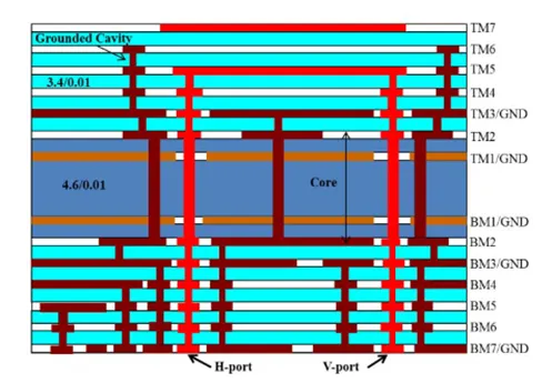
Figure 3. HDI stack structure
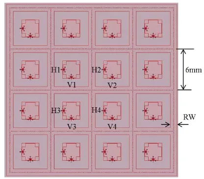
Figure 4. Patch array antenna
To meet heterogeneous integration requirements, packaged antenna implementation must adapt to advanced packaging processes and exploit their advantages. Current 2.5D/3D packaging approaches are volumetric and make efficient use of chip area and height; they reduce interconnect length compared with traditional packaging and improve signal transmission speed.
In advanced packaging, different interposer materials offer distinct advantages and target applications. Interposer materials commonly fall into three categories: silicon, glass, and organic materials.
Silicon interposers
Silicon interposers are widely used due to mature silicon processing. They can use wafer-level routing processes similar to those on IC wafers, enabling narrower traces, smaller spacing, higher routing density, and improved reliability compared with traditional substrates. In silicon-interposer-based 2.5D/3D packages, vertical interconnects use TSVs and RDLs handle planar system interconnects. Interconnect loss is a critical factor for millimeter-wave AiP, and advanced processing can enable direct interconnection between antenna and chip, reducing size and signal crosstalk. In 2022, Y. Huang and collaborators proposed a W-band backed-cavity antenna using silicon interposer multilayer routing with a BCB-based MEMS photosensitive composite thin-film process for low-loss interconnects while maintaining high gain and impedance bandwidth. The design uses high-resistivity silicon substrates and is suitable for AiP implementations (Figure 5).
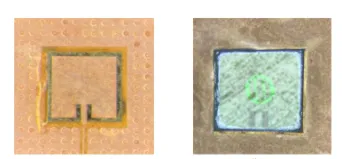
Figure 5. Packaged antenna with BCB material interconnects
Glass interposers
Glass interposers have high resistivity and low dielectric constant, making them attractive for RF applications. They also offer strong mechanical stability, low warp, and relatively low cost. Through-glass vias (TGVs) enable 2.5D/3D integration on glass, but current process limitations result in TGV aspect ratios and via-wall roughness that lag behind TSVs, constraining large-scale adoption until these issues are addressed. For example, a 2022 design by Y. Su et al. presented a 77 GHz automotive radar antenna using TGVs for layer interconnection. The antenna comprises five glass layers and six metal layers, and the wafer and stack-based fabrication improves routing capability for complex antenna designs (Figure 6).
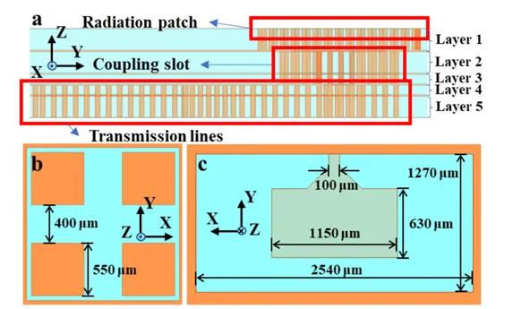
Figure 6. Automotive radar antenna implemented with a five-layer glass stack
Organic interposers
Organic materials such as PTFE (polytetrafluoroethylene), LCP (liquid crystal polymer), and PI (polyimide) are also used as interposers. Compared with traditional boards like FR4, organic interposers attract attention in millimeter-wave bands due to lower loss tangent. In 2023, H. Araki et al. reported an AiP structure using a novel low-dielectric-constant, low-loss-tangent PI material as the interposer (Figure 7), achieving lower transmission loss compared with conventional PI and improving suitability for millimeter-wave AiP.
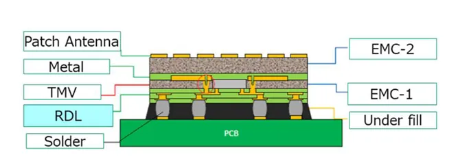
Figure 7. Packaged antenna using a novel PI interposer material
Conclusion
In heterogeneous integration, packaged antennas are a key component for efficient millimeter-wave communication. Effective AiP design requires coordinated consideration of antenna topology, packaging processes, and material choices to meet practical application requirements.