ALLPCB


What is IC design
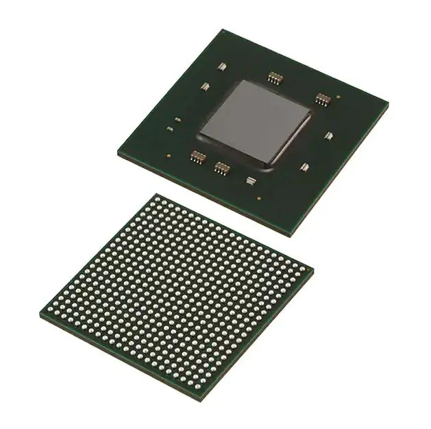
IC design is a common term for chip design. IC stands for Integrated Circuit and is also referred to as a chip. IC design is the process of designing an integrated circuit as a whole, including circuit design, placement and routing, and physical design.
In IC design, engineers use EDA tools to design and simulate various circuits, such as logic circuits, analog circuits, and digital signal processing blocks. Based on the specification requirements, they perform placement and routing to determine component locations and interconnects. Finally, physical design addresses issues such as electromagnetic compatibility, power optimization, and timing, and produces the mask data required for chip fabrication.
IC design is the core part of chip development. It spans circuit design, layout, and physical implementation, aiming to integrate multiple functional circuits into a small chip to achieve high integration, high performance, and low power.
Digital IC design flow
The typical digital IC design flow includes the following main steps:
- Specification definition: Define the chip's functional specifications, performance targets, and interface requirements based on application needs.
- Architecture design: Design the overall chip structure, including the partitioning and organization of signal processing, control logic, and memory modules.
- RTL design: Describe the chip functionality at the register transfer level using hardware description languages such as Verilog or VHDL. RTL design includes logical design and functional simulation.
- Synthesis and optimization: Synthesize RTL into a gate-level netlist and perform optimizations to meet performance, power, and area targets.
- Placement and routing: Perform placement according to the optimized netlist, determine module locations and sizes, and complete routing to establish interconnections.
- Physical verification: Run design rule checking (DRC) and layout versus schematic (LVS) checks and other physical verification to ensure the layout meets foundry rules and design constraints.
- Static timing analysis: Perform static timing analysis, set timing constraints, partition clock domains, and verify timing convergence to ensure timing requirements are met.
- Dynamic simulation: Run functional and timing simulations to validate design correctness and performance.
- Test integration: Design and integrate on-chip test circuits and test interfaces for subsequent chip testing and fault diagnosis.
- Final layout: Produce the final layout, including metal layer planning and design rule settings.
- Analog simulation and verification: Simulate and verify any analog circuitry within the design to ensure performance and stability.
- Fabrication: Submit the finished layout to a foundry for chip fabrication and packaging.
Common digital IC design tools
Common tools used in digital IC design include:
- RTL design: Vivado, Quartus, Design Compiler front-ends.
- Synthesis: Synopsys Design Compiler, Cadence Genus, DC Compiler.
- Place and route: Cadence Innovus, ICC, Olympus-SoC.
- Physical verification: Mentor Calibre, Synopsys StarRC, IC Validator.
- Software simulation: ModelSim, VCS, Incisive.
- Analog simulation: Cadence Spectre, HSPICE, Cadence Virtuoso.
Specific tool choices vary depending on the design team and flow. The tools listed above are common examples, not an exhaustive list.
Design versus verification
Design and verification are both essential parts of the digital IC design flow and are mutually dependent. They have different goals and responsibilities.
Design covers architecture, logic, and physical implementation, aiming to realize the functionality and performance defined in the specification through module design, placement, and routing.
Verification validates the design's functionality and characteristics throughout the design process to ensure correctness and that performance targets are met. Verification includes functional simulation, timing simulation, and analog simulation to detect errors and verify stability.
Good design provides the foundation for verification, and good verification confirms that the design meets its objectives and uncovers issues for correction. Both are critical to producing a reliable, high-quality chip design; neither can be considered more important in isolation.