ALLPCB


If you've ever worked on a printed circuit board (PCB) and accidentally lifted a solder pad, you know how frustrating it can be. A lifted solder pad can disrupt electrical connections and render a board unusable if not addressed properly. But don't worry—repairing lifted solder pads is entirely possible with the right tools and techniques. In this practical guide, we'll walk you through everything you need to know about handling lifted solder pads, from understanding why they happen to step-by-step repair methods for effective solder pad repair.
Whether you're a hobbyist or a professional engineer, this blog will equip you with actionable tips and insights to tackle soldering challenges and restore your PCB to full functionality. Let’s dive into the world of lifted solder pads and learn how to fix them with confidence.
What Are Lifted Solder Pads and Why Do They Happen?
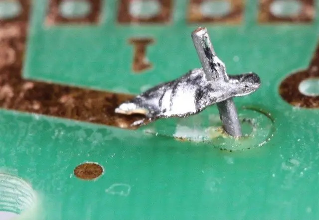
A solder pad is a small area of copper on a PCB where components are attached using solder. When a solder pad becomes detached from the board—either partially or completely—it’s referred to as a "lifted solder pad." This issue can break the electrical connection between components, causing a circuit to fail.
Understanding why solder pads lift is the first step to preventing and repairing them. Here are the most common causes:
- Excessive Heat: Applying too much heat during soldering or desoldering can weaken the adhesive bond between the copper pad and the PCB substrate, causing the pad to lift. For instance, using a soldering iron above 350°C (662°F) for extended periods can damage the board.
- Mechanical Stress: Physically pulling or twisting a component while desoldering can tear the pad off the board. This often happens when components are soldered too tightly or removed without proper care.
- Poor PCB Quality: Low-quality boards with thin copper layers or weak adhesion are more prone to pad lifting. Boards with copper thickness below 1 oz/ft2 are particularly vulnerable.
- Overworking the Joint: Repeated soldering and desoldering on the same pad can weaken its bond with the board, eventually leading to lifting.
By identifying the root cause of a lifted pad, you can take steps to avoid similar issues in the future and approach the repair with a clear strategy.
Tools and Materials Needed for Solder Pad Repair
Before attempting to fix a lifted solder pad, gather the right tools and materials. Having everything ready will make the process smoother and reduce the risk of further damage. Here’s what you’ll need:
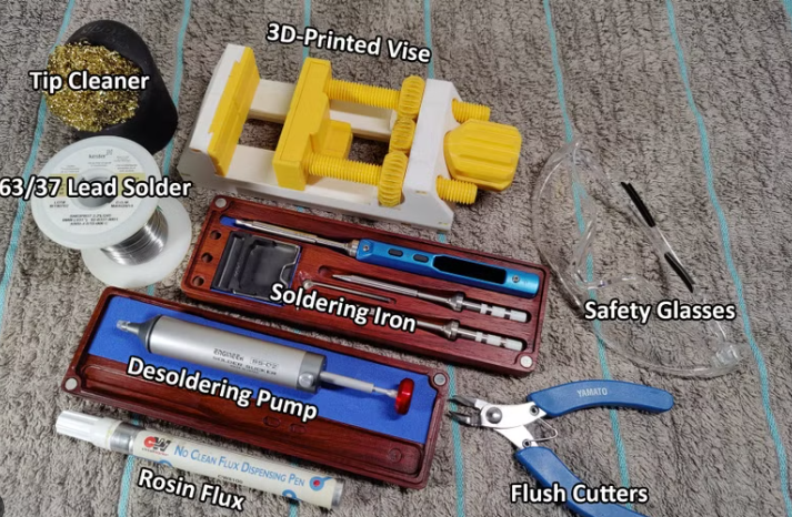
- Temperature-Controlled Soldering Iron: A fine-tip iron (15-30 watts) allows precise control over heat, preventing additional damage to the board. Set it to around 300°C (572°F) for most repairs.
- Solder: Use high-quality, flux-core solder, ideally lead-free for modern electronics. A diameter of 0.5mm to 0.8mm works well for small repairs.
- Desoldering Braid or Solder Wick: This helps remove excess solder from the damaged area.
- Flux: Liquid or gel flux improves solder flow and adhesion, ensuring a strong connection.
- Replacement Pads (if needed): If the pad is completely torn off, you may need a copper foil or replacement pad from an electronics supplier.
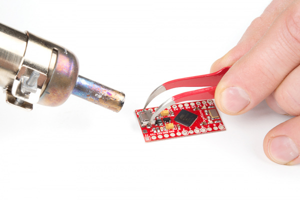
- Magnifying Glass or Microscope: Small pads are hard to see with the naked eye, so magnification helps with precision.
- Tweezers: Useful for handling small components and wires during repair.
- Isopropyl Alcohol and Brush: Clean the area after repair to remove residue and prevent corrosion.
With these tools in hand, you're ready to tackle the repair process. Always ensure your workspace is well-lit and ventilated to maintain safety and visibility.
Related Reading: Essential Tools for ECU PCB Repair: A DIY Guide
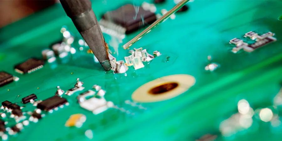
Step-by-Step Guide to Repairing Lifted Solder Pads
Repairing a lifted solder pad requires patience and precision, but it’s a skill worth mastering. Follow these steps to restore your PCB effectively:
Step 1: Assess the Damage
Start by closely inspecting the lifted pad under magnification. Determine whether the pad is partially lifted (still partially attached to the board) or completely torn off. Also, check if the underlying trace—a thin copper line connecting pads—is still intact. This will guide your repair approach.
Step 2: Clean the Area
Use a desoldering braid or solder wick to remove any old solder from the damaged pad and surrounding area. Apply a small amount of flux to help the solder flow away from the pad. Then, clean the area with isopropyl alcohol and a brush to remove debris or residue. A clean surface ensures better adhesion during repair.
Step 3: Secure a Partially Lifted Pad
If the pad is partially lifted, you may be able to reattach it. Apply a small amount of flux to the pad and the board underneath. Gently press the pad back into place using tweezers. Heat the pad with your soldering iron and apply a thin layer of fresh solder to bond it to the board. Avoid overheating—limit contact to 2-3 seconds at a time.
Step 4: Replace a Completely Torn Pad
If the pad is completely gone, you’ll need to create a new connection point. One option is to use a small piece of copper foil or a replacement pad. Cut the foil to match the size of the original pad (typically 1-2mm in diameter for small components). Apply flux to the board and the foil, then solder the foil in place over the trace. Ensure it makes solid contact with the underlying copper trace.
Step 5: Connect the Component
Once the pad is secured or replaced, solder the component lead to the pad. If the original trace is damaged or inaccessible, you may need to run a small jumper wire (e.g., 30 AWG wire) from the pad to the next connection point in the circuit. Refer to the PCB schematic to identify the correct connection point. Solder the wire carefully to avoid creating shorts.
Step 6: Test the Repair
After completing the repair, visually inspect the area for any loose connections or solder bridges. Use a multimeter to test for continuity between the repaired pad and other points in the circuit. If the connection is stable and the circuit functions as expected, your repair is successful.
Related Reading: Repairing Lifted Pads: A Comprehensive Guide for Engineers
Tips for Preventing Lifted Solder Pads During Soldering
While knowing how to repair lifted solder pads is valuable, preventing the issue in the first place is even better. Here are practical tips to minimize the risk during soldering:
- Control Heat: Use a temperature-controlled soldering iron and keep the temperature between 280°C and 320°C (536°F-608°F) for most PCBs. Avoid prolonged contact with the pad—limit it to 3-5 seconds per joint.
- Use Flux: Applying flux before soldering helps the solder flow smoothly, reducing the need for excessive heat or rework.
- Be Gentle with Components: When desoldering, use a desoldering braid or pump to remove solder before gently lifting the component. Avoid pulling or twisting, as this can stress the pad.
- Work on Stable Surfaces: Ensure your PCB is secured on a flat, stable surface to prevent accidental movement that could damage pads.
- Practice on Scrap Boards: If you’re new to soldering, practice on old or scrap PCBs to build your skills before working on critical projects.
By following these precautions, you can significantly reduce the chances of encountering lifted solder pads in your projects.
Advanced Techniques for Complex Solder Pad Repairs
For more challenging scenarios, such as lifted pads on multilayer boards or pads connected to high-frequency traces, advanced techniques may be necessary. Here are a few approaches for experienced users:
- Trace Repair: If the copper trace connected to the pad is damaged, carefully scrape away the solder mask (the green coating on the PCB) using a fine blade to expose the trace. Solder a thin wire to reconnect the pad to the trace. For high-frequency circuits, ensure the wire length is minimized to avoid impedance mismatches, ideally keeping it under 5mm for signals above 100 MHz.
- Epoxy Reinforcement: After repairing a lifted pad, apply a small amount of PCB-grade epoxy over the pad to strengthen its bond with the board. This is particularly useful for pads that will experience mechanical stress.
- Professional Tools: For intricate repairs, consider using a hot air rework station to evenly heat the area without direct contact. This can prevent further damage to delicate pads.
These techniques require a steady hand and a deep understanding of PCB design, so proceed with caution if you’re not experienced in advanced repairs.
Common Mistakes to Avoid When Repairing Lifted Solder Pads
Even with the best intentions, mistakes can happen during solder pad repair. Here are some common pitfalls to watch out for:
- Overheating the Board: Excessive heat can cause further lifting or damage nearby components. Always monitor your soldering iron temperature and limit contact time.
- Using Too Much Solder: Excess solder can create bridges between pads, leading to short circuits. Use just enough solder to form a secure, shiny joint—typically a small dome covering the pad.
- Ignoring the Schematic: When running jumper wires, always refer to the circuit schematic to ensure you’re connecting to the correct point. Incorrect connections can cause circuit failure.
- Skipping Cleaning: Failing to clean the area after repair can leave flux residue, which may corrode the board over time. Always clean with isopropyl alcohol after soldering.
Avoiding these mistakes will improve the quality of your repairs and extend the lifespan of your PCB.
When to Seek Professional Help for Solder Pad Repair
While many lifted solder pad issues can be fixed at home or in a workshop, some situations call for professional assistance. Consider seeking help if:
- The PCB is part of a high-value or critical system, such as medical or industrial equipment.
- The board has multiple layers, and internal traces are damaged, requiring specialized equipment to repair.
- You’ve attempted a repair but the circuit still doesn’t function, indicating a deeper issue.
Professional repair services have access to advanced tools and expertise, ensuring the board is restored without risking further damage.
Conclusion: Mastering Solder Pad Repair for Reliable PCBs
Handling lifted solder pads doesn’t have to be a daunting task. With the right tools, techniques, and a bit of patience, you can repair damaged pads and bring your PCB back to life. From assessing the damage to applying advanced repair methods, this guide has covered the essentials of solder pad repair and soldering best practices. Remember to prioritize prevention by controlling heat, using flux, and handling components with care during soldering projects.
By mastering these skills, you’ll not only save time and money but also build confidence in tackling a wide range of PCB issues. Keep practicing, stay equipped with quality tools, and approach each repair with precision. Your ability to handle lifted solder pads will ensure your electronics projects remain reliable and functional for years to come.