ALLPCB


1. Introduction
GaN-based optoelectronic devices and HEMT power devices often face challenges during fabrication such as layer release and thermal management. Heteroepitaxy using 2D materials like graphene, diamond, and h-BN can mitigate thermal mismatch and enable transfer of GaN layers. Conventional GaN heteroepitaxy is typically performed on sapphire, Si, or SiC substrates; release from sapphire in particular is difficult, causing significant material loss and extra cost, and release technologies require further improvement. Heteroepitaxy on 2D materials such as graphene offers a route to easier layer release.
2. Growth of GaN on 2D Materials
The following examples illustrate methods to grow GaN on 2D materials such as graphene.
(1) Sapphire / Graphene / GaN
In merged regions of the GaN film, stepped surface morphologies are observed. RMS values are 0.113 and 0.142 nm, respectively.
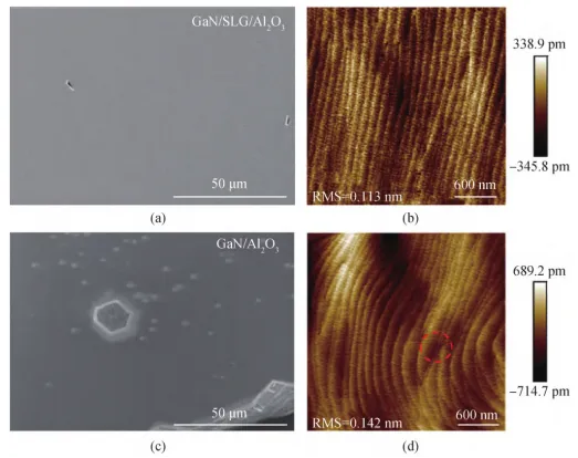
Figure 1: SEM (a, c) and AFM (b, d) images for GaN/SLG/Al2O3 and GaN/Al2O3.
GaN films grown on graphene show lower RMS and a smoother surface, which may be attributed to enhanced lateral coalescence of GaN on graphene. A small number of dislocations were observed in the GaN/Al2O3 system, likely screw or mixed dislocations.
The dashed box in Figure 2 contains a high-resolution TEM image of the interface where the graphene layer is clearly visible.
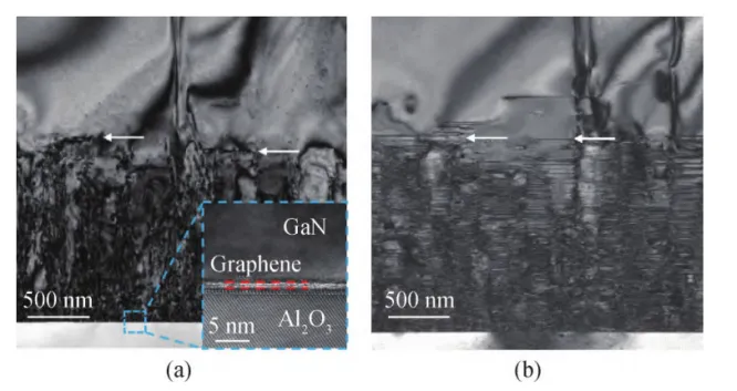
Notably, many basal plane stacking faults (SFs) are present in the nucleation layer during the initial growth stage, as shown in Figure 2(b). A large number of dislocations are blocked at the locations where these basal plane SFs appear. These short-range SFs act as masks during GaN growth and inhibit the vertical propagation of dislocations, resulting in a relatively low dislocation density in the GaN film above.
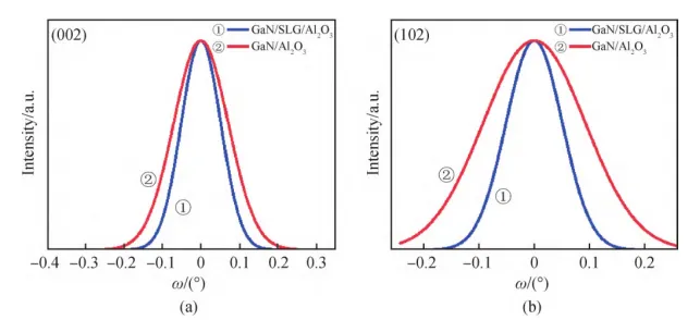
XRD data in Figure 3 show 002 and 102 peak positions for sapphire/graphene/GaN at 418.6 and 601.6, respectively. From the calculations, the screw dislocation density is 6.63 x 10^8 cm^-2 and the edge dislocation density is 1.37 x 10^9 cm^-2, indicating that graphene helps relax lattice mismatch and reduce dislocation density.
(2) Sapphire / Graphene / AlN buffer / GaN
Direct growth of GaN on graphene can suffer from insufficient nucleation due to the lack of dangling bonds on the graphene surface, and NH3 used as the nitrogen source can etch graphene, compromising its integrity. To address this, an AlN buffer layer can be deposited (for example by sputtering) to increase GaN nucleation density and to protect graphene from NH3 etching.
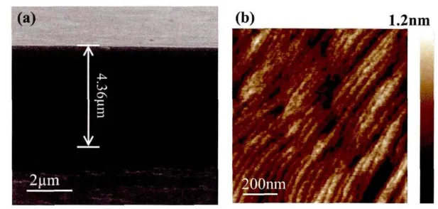
Figure 4 shows a GaN film with a thickness of 4.36 μm. The AFM topology reveals clear atomic steps and a relatively smooth surface.
(3) Sapphire / h-BN / GaN
Hexagonal boron nitride (h-BN) is a III-group nitride-like 2D material with hexagonal crystal symmetry. Compared with graphene, h-BN is more compatible with the epitaxial growth of III-nitrides such as GaN and offers better oxidation resistance, reducing oxygen impurity incorporation in epitaxial GaN films. h-BN also has good high-temperature stability and notable mechanical flexibility, making it a suitable 2D transition layer between substrate and GaN epitaxial film.
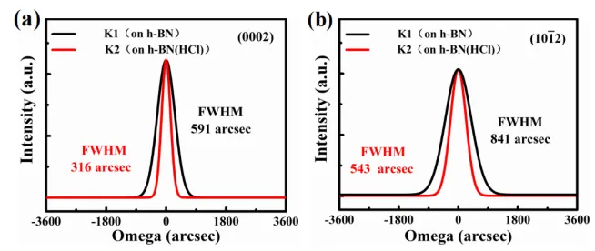
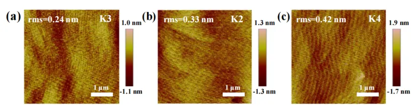
By optimizing sapphire/h-BN composite substrates and h-BN thickness, GaN films were obtained on these substrates. Figure 5 shows XRD data and Figure 6 shows AFM data for different samples.
3. Industrial Applications
Growing GaN on 2D materials can reduce dislocations and stress between the epitaxial film and substrate caused by lattice and thermal mismatch. With advances in 2D material fabrication, 2D crystals can be introduced as transition layers between substrate and film during epitaxy, providing a new route for GaN heteroepitaxy.
2D materials can be single-atom or few-atom layers thick and include zero-bandgap graphene, wide-bandgap h-BN, transition metal dichalcogenides (MoS2, WS2, etc.), and oxides (MoO3, WO3, etc.).
In industry, this approach can facilitate development of nitride material and device layer release and transfer processes, enabling transferable GaN-based device structures. It also offers potential advantages for device thermal management.