 ALLPCB


Preface
Most designers are familiar with Pierce topology oscillators, but few fully understand how they work or how to design them correctly. Oscillator issues are often overlooked until production, causing delays or operational problems. Oscillators should receive appropriate attention during the design phase and before production.
Quartz Crystal Characteristics and Equivalent Model
A quartz crystal is a piezoelectric device that converts electrical energy to mechanical energy and vice versa at its resonance frequency. It can be represented by the following equivalent circuit:
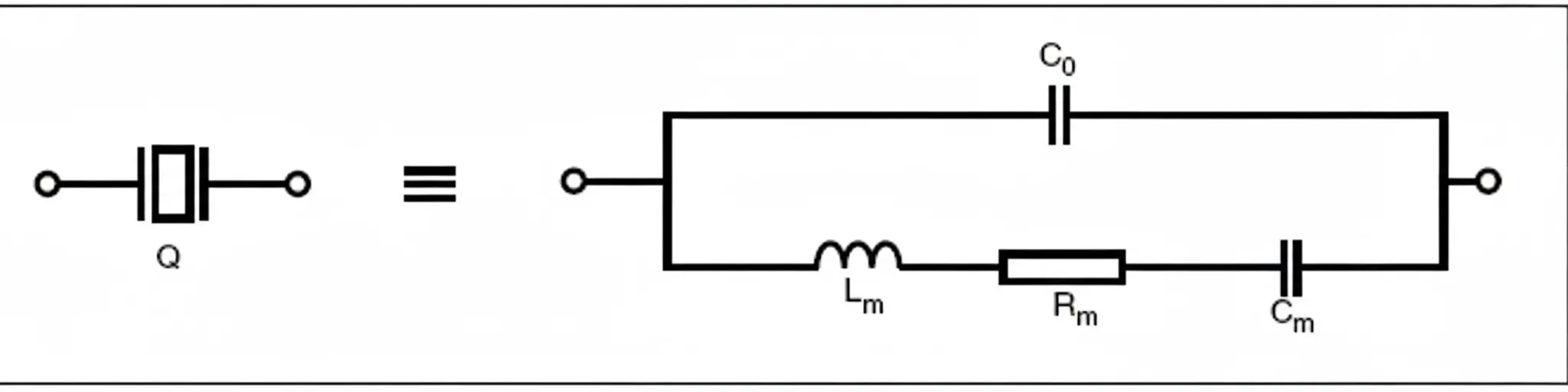
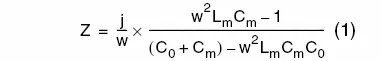
The crystal impedance can be expressed by the following equation (assuming Rm is negligible):
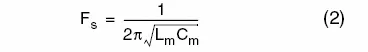
Fs is the series resonance frequency where reactance Z = 0 (it is the resonance of the Lm, Cm and Rm branch). Its expression is:
The range from Fs to Fa is commonly called the parallel-resonance region (shaded in the figure). In this region the crystal operates in parallel resonance (this is the normal operating region; Fa ? Fs is the bandwidth. Narrower bandwidth implies higher Q and more stable oscillation frequency). In this region the crystal presents an inductive characteristic, producing approximately 180° phase shift. The oscillation frequency FP (also called FL: load frequency) is given by:

From this expression, it is clear that the oscillation frequency can be tuned by adjusting the load capacitance CL. This is why crystal vendors specify an external load capacitance CL in their datasheets. Specifying CL ensures the crystal oscillates at its nominal frequency.
Example: Adjusting External Parameters for an 8 MHz Crystal
Using the previous expressions, the crystal's Fs, Fa and FP were calculated as: Fs = 7,988,768 Hz, Fa = 8,008,102 Hz. If the crystal's CL is 10 pF, the oscillation frequency is FP = 7,995,695 Hz. To reach the 8 MHz nominal frequency, CL should be 4.02 pF.
Oscillator Principle
An oscillator consists of an amplifier and a feedback network that provides frequency selection. The block diagram illustrates the basic principle:
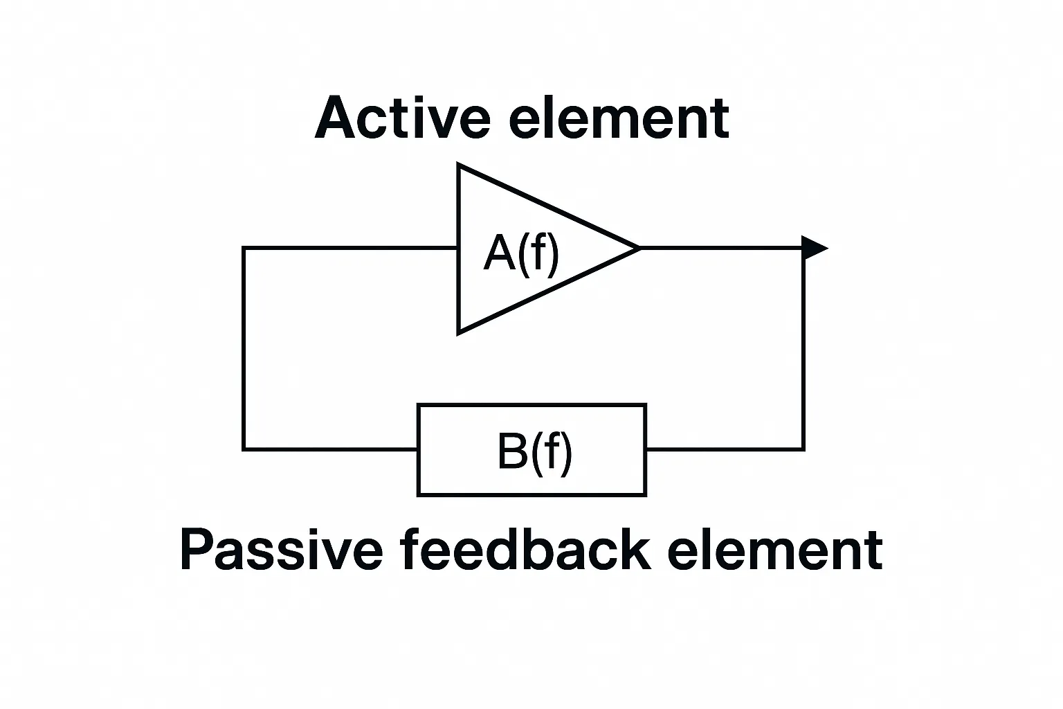
- A(f) is the amplifier section, which supplies energy to sustain oscillation.
- B(f) is the feedback path, which determines the oscillation frequency.
To start oscillation, the Barkhausen conditions must be met: the closed-loop gain should be greater than 1 and the total phase shift should be 360°.
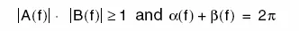
To sustain oscillation, ensure |A(f)|·|B(f)| >> 1. This implies the open-loop gain should be much greater than 1; the time to reach steady oscillation depends on that open-loop gain.
However, satisfying these conditions alone does not explain how a crystal oscillator starts. A startup energy source is also required. In practice, power-up transients and noise provide the necessary energy. The startup energy must be sufficient to excite oscillation at the desired frequency.
The amplifier in this condition is unstable, so any disturbance in the positive feedback loop can trigger oscillation. Disturbances can come from power-up events, device enable/disable actions, crystal thermal noise, and so on. Note that only noise components within the crystal's operating frequency range are amplified; this is why crystal oscillators can require significant time to start.
Pierce Oscillator
The Pierce oscillator is common due to its low power, low cost and good stability.
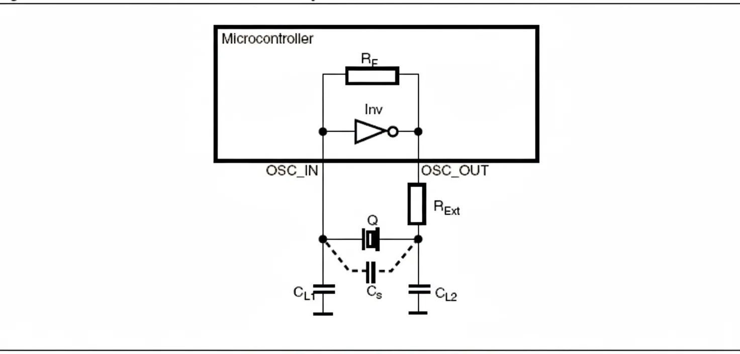
- Inv: internal inverter acting as the amplifier.
- Q: quartz or ceramic resonator.
- RF: internal feedback resistor. Its presence biases the inverter into the linear region so it provides gain equivalent to an amplifier.
- RExt: external current-limiting resistor.
- CL1 and CL2: two external load capacitors.
- Cs: stray capacitance from PCB traces and connections at OSC_IN and OSC_OUT pins.
Pierce Oscillator Design
Feedback Resistor RF
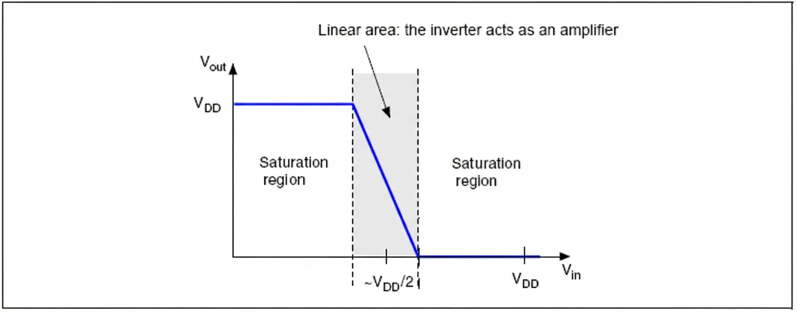
In many cases RF is embedded inside the oscillator circuit (for example, inside many microcontrollers). Its role is to introduce feedback that makes the inverter operate as an amplifier.
The feedback resistor between Vin and Vout biases the inverter when Vout = Vin, forcing the inverter to operate in its linear region (shaded area in the figure). The amplifier then amplifies noise within the crystal's parallel-resonance region (e.g. crystal thermal noise), which triggers startup. In some cases, after startup the oscillator may continue to run even if RF is removed.
Load Capacitance CL
Load capacitance CL refers to the effective capacitance seen by the crystal. CL depends on the external capacitors CL1 and CL2 and the PCB stray capacitance Cs. The crystal manufacturer specifies the CL value required to achieve the nominal frequency. Frequency accuracy depends on matching the circuit load capacitance to the specified value, while frequency stability depends on keeping the load capacitance constant. External capacitors CL1 and CL2 are used to adjust CL to the manufacturer's specified value. The effective CL is:
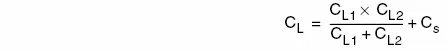
Example calculation for CL1 and CL2: if CL = 15 pF and assume Cs = 5 pF, then:
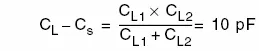
Thus CL1 = CL2 = 20 pF.
Gain Margin of the Oscillator
Gain margin is a key parameter that determines whether the oscillator will reliably start.
Where:
- gm is the inverter transconductance, in mA/V for high frequency or μA/V for low frequency (e.g. 32 kHz).
- gmcrit (critical gm) depends on the crystal parameters. Assuming CL1 = CL2 and that the crystal sees the manufacturer-specified CL, gmcrit is:
ESR is the crystal equivalent series resistance. According to the theory by Eric A. Vittoz et al. (see "High-Performance Crystal Oscillator Circuits: Theory and Application", IEEE Journal of Solid-State Circuits, vol. 23, No. 3, pp. 774-782, Jun. 1988), the impedances of the amplifier and the two external capacitors compensate the reactance of the crystal's RLC dynamic equivalent circuit.
To satisfy startup conditions, the inverter transconductance must meet gm > gmcrit.


