ALLPCB


In the world of high-speed circuits, ensuring signal integrity is a top priority for PCB designers. One of the most effective techniques to achieve this is controlled depth drilling, often referred to as back drilling. But what exactly is controlled depth drilling, and how does it help in minimizing reflections in PCB design? In short, controlled depth drilling removes unused portions of vias, known as via stubs, which can cause signal reflections and degrade performance in high-speed circuits. By eliminating these stubs, designers can optimize signal integrity and ensure reliable data transmission.
This blog post will dive deep into the concept of controlled depth drilling, its role in maintaining signal integrity, and how it minimizes reflections in PCB design. We'll explore the technical details, benefits, and best practices for high-speed circuits, providing actionable insights for engineers and designers looking to enhance their projects. Let’s get started!
What is Controlled Depth Drilling in PCB Design?
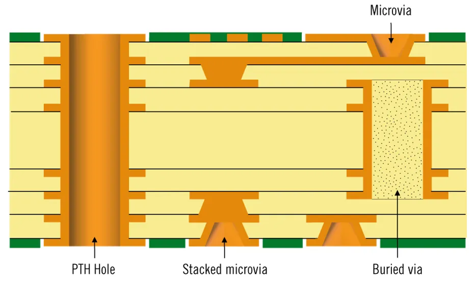
Controlled depth drilling, commonly known as back drilling, is a manufacturing process used in printed circuit board (PCB) production. It involves drilling into a PCB from the opposite side of a plated through-hole (PTH) via to remove the unused portion of the via, often called a via stub. These stubs are leftover copper segments that do not carry any signal but can interfere with high-speed signals by causing reflections.
In high-speed circuits, where data rates can exceed 10 Gbps, even small imperfections like via stubs can lead to significant signal distortion. Back drilling targets these stubs by using a slightly larger drill bit to remove the conductive material without affecting the functional part of the via. This process ensures that only the necessary portion of the via remains, reducing unwanted electrical effects.
Why Signal Integrity Matters in High-Speed Circuits
Signal integrity refers to the quality of an electrical signal as it travels through a PCB. In high-speed circuits, maintaining signal integrity is critical because any distortion or interference can lead to data errors, reduced performance, or complete system failure. Common issues that affect signal integrity include crosstalk, noise, and reflections.
Reflections occur when a signal encounters an impedance mismatch, such as at the end of a via stub. This mismatch causes part of the signal to bounce back, interfering with the original signal. In high-speed designs operating at frequencies above 1 GHz, these reflections can create significant problems, including signal delay and loss of data integrity. For example, a via stub as short as 0.5 mm can cause noticeable reflections at 5 Gbps data rates, leading to bit errors.
By addressing these issues through techniques like controlled depth drilling, designers can ensure cleaner signal transmission and better overall performance in applications like telecommunications, data centers, and advanced computing systems.
How Via Stubs Cause Reflections in PCB Design
To understand the importance of back drilling, it’s essential to know how via stubs contribute to reflections. In a multilayer PCB, vias are used to connect traces on different layers. When a via extends beyond the layer where the signal is needed, the unused portion becomes a via stub. This stub acts like an unterminated transmission line, creating an impedance discontinuity.
When a high-speed signal passes through the via, part of the energy reflects back from the stub due to this mismatch. The reflected signal interferes with the original signal, causing distortion. The longer the via stub, the more pronounced the reflection becomes. For instance, at a data rate of 10 Gbps, a stub length of 1 mm can result in a reflection loss of up to 3 dB, significantly degrading the signal.
Controlled depth drilling eliminates these stubs, ensuring that the via length matches the signal path, thus minimizing reflections and maintaining signal integrity.
The Process of Controlled Depth Drilling
Back drilling is a precise manufacturing technique that requires careful planning and execution. Here’s a step-by-step overview of how it works:
- Design Planning: During the PCB design phase, engineers identify vias that require back drilling based on signal paths and layer transitions. Design software often includes tools to mark these vias for manufacturing.
- Initial Drilling: The PCB undergoes standard drilling to create plated through-hole vias as part of the multilayer stack-up.
- Back Drilling: A secondary drilling process is performed from the opposite side of the PCB using a slightly larger drill bit (typically 0.2 mm larger than the original via diameter). This removes the unused copper stub without damaging the functional part of the via.
- Inspection: After drilling, the PCB is inspected to ensure that the stub has been removed accurately and that no debris or damage affects the via’s integrity.
The precision of controlled depth drilling is critical. If the drill goes too deep, it can damage the signal-carrying portion of the via. If it’s too shallow, the stub remains, and reflections persist. Modern manufacturing equipment can achieve depth tolerances as tight as ±0.05 mm, ensuring reliable results.
Benefits of Back Drilling for Signal Integrity
Controlled depth drilling offers several advantages for high-speed PCB designs, making it a preferred choice for engineers working on cutting-edge technologies. Here are the key benefits:
- Reduced Reflections: By removing via stubs, back drilling eliminates the primary source of signal reflections, ensuring cleaner transmission at high frequencies.
- Improved Signal Integrity: With fewer reflections and distortions, signal quality improves, reducing bit error rates in high-speed circuits operating at 10 Gbps or higher.
- Lower Crosstalk: Removing stubs also reduces electromagnetic interference between adjacent vias, minimizing crosstalk in densely packed designs.
- Enhanced Performance: Applications like 5G, data centers, and high-performance computing benefit from the improved reliability and speed that back drilling provides.
- Cost-Effective Solution: While back drilling adds a step to the manufacturing process, it is often more affordable than redesigning a PCB or using more complex via structures like blind or buried vias.
Design Guidelines for Effective Back Drilling
To maximize the benefits of controlled depth drilling, PCB designers must follow specific guidelines during the design and manufacturing phases. Here are some best practices to ensure optimal results:
1. Identify Critical Vias Early
During the schematic and layout stages, identify which vias carry high-speed signals and are likely to have stubs. Focus back drilling efforts on these critical paths to avoid unnecessary costs.
2. Specify Drill Depths Precisely
Work closely with your manufacturing partner to define exact drill depths for each via. Provide detailed documentation, including stack-up information and target layers, to avoid errors. A typical tolerance for drill depth is ±0.1 mm, but tighter tolerances may be needed for advanced designs.
3. Minimize Stub Length in Design
Where possible, route signals to minimize via stub length even before back drilling. For instance, transitioning signals to inner layers closer to the via entry point reduces the stub size.
4. Use Appropriate Via Sizes
Choose via diameters that balance signal requirements with manufacturing capabilities. Smaller vias may limit the size of the back drill bit, while larger vias can affect board density. A common via diameter for high-speed designs is 0.3 mm, with a back drill diameter of 0.5 mm.
5. Test and Validate
After manufacturing, use tools like time-domain reflectometry (TDR) to measure impedance and confirm that reflections have been minimized. For a 50-ohm transmission line, post-back drilling impedance should remain within ±5% of the target value.
Challenges and Limitations of Controlled Depth Drilling
While back drilling is highly effective, it’s not without challenges. Understanding these limitations can help designers make informed decisions:
- Manufacturing Complexity: Back drilling adds an extra step to the production process, increasing lead times and costs, especially for large-scale projects.
- Precision Requirements: Achieving accurate drill depths in multilayer boards with 16 or more layers can be difficult, requiring advanced equipment and skilled operators.
- Not Suitable for All Designs: For low-speed circuits or designs with minimal via stubs, back drilling may be unnecessary and cost-prohibitive.
- Potential for Damage: If not executed correctly, back drilling can damage nearby traces or vias, leading to electrical failures.
Despite these challenges, the benefits of controlled depth drilling often outweigh the drawbacks for high-speed applications where signal integrity is non-negotiable.
Applications of Back Drilling in High-Speed Circuits
Controlled depth drilling is widely used in industries that rely on high-speed data transmission. Some key applications include:
- Telecommunications: In 5G infrastructure, where data rates exceed 25 Gbps, back drilling ensures minimal signal loss and reflections in base station equipment.
- Data Centers: Servers and networking hardware require pristine signal integrity to handle massive data throughput, often at speeds of 56 Gbps or more.
- Aerospace and Defense: High-reliability systems, such as radar and avionics, use back drilling to maintain signal quality in harsh environments.
- Consumer Electronics: Devices like high-end gaming consoles and VR headsets benefit from back drilling to support fast, error-free data transfer.
Future Trends in Signal Integrity and PCB Design
As data rates continue to climb—think 100 Gbps and beyond—the demand for advanced signal integrity solutions like controlled depth drilling will only grow. Innovations in manufacturing technology are making back drilling more precise and cost-effective, while design software now offers better simulation tools to predict and mitigate reflections before production.
Additionally, emerging techniques like microvia technology and hybrid stack-ups are complementing back drilling, offering designers more options to tackle signal integrity challenges. Staying ahead of these trends ensures that your PCB designs remain competitive in a rapidly evolving industry.
Conclusion: Optimizing Signal Integrity with Controlled Depth Drilling
In the realm of high-speed circuits, maintaining signal integrity is paramount, and controlled depth drilling offers a proven solution to minimize reflections. By removing via stubs through back drilling, designers can eliminate a major source of signal distortion, ensuring reliable performance in applications ranging from 5G networks to data centers.
Understanding the process, benefits, and best practices of back drilling empowers engineers to create PCBs that meet the stringent demands of modern electronics. Whether you're working on a complex multilayer design or optimizing a high-frequency circuit, incorporating controlled depth drilling into your workflow can make all the difference.
With the right design approach and manufacturing partnership, achieving optimal signal integrity is within reach. Embrace the power of back drilling, and take your PCB designs to the next level!