ALLPCB


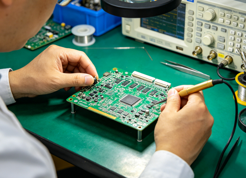
In the fast-evolving world of electronics, designing a printed circuit board (PCB) that performs reliably under complex conditions is a critical skill. For engineers and designers working on sophisticated projects, mastering advanced PCB routing techniques and multi-layer PCB design is essential. This blog post dives deep into the intricacies of multi-layer PCB stackup design, blind and buried vias in PCB, impedance control routing, differential pair routing techniques, and high-density interconnect PCB routing. Whether you're optimizing signal integrity or tackling high-speed designs, these strategies will elevate your PCB layouts to the next level.
At its core, advanced PCB routing ensures that signals travel efficiently across multiple layers without interference, noise, or performance loss. By understanding and applying the techniques discussed here, you can create compact, powerful, and reliable designs for modern devices. Let’s explore each aspect in detail to help you achieve optimal results in your next project.
Understanding Multi-Layer PCB Stackup Design
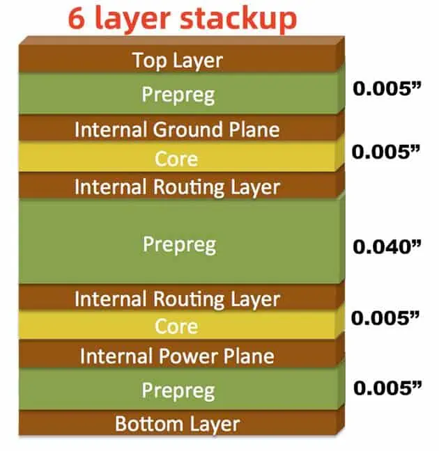
A multi-layer PCB consists of several layers of conductive material separated by insulating layers, allowing for more complex and compact designs. The arrangement of these layers, known as the multi-layer PCB stackup design, plays a pivotal role in determining the board’s performance, especially for high-speed and high-density applications.
A typical stackup for a 6-layer PCB might include two signal layers on the top and bottom, with internal layers dedicated to power and ground planes. This configuration helps reduce electromagnetic interference (EMI) by providing a stable reference plane for signals. For instance, placing a ground plane adjacent to a signal layer can reduce crosstalk by up to 50% in high-speed designs operating at frequencies above 100 MHz.
When designing a stackup, consider the following:
- Layer Count: Determine the number of layers based on component density and routing needs. A 10-layer board, for example, might be necessary for a design with multiple high-speed signals requiring dedicated planes.
- Material Selection: Use materials with appropriate dielectric constants (Dk) to control signal speed. For high-frequency designs, materials like FR-4 (Dk ≈ 4.5) may be replaced with low-loss alternatives like Rogers (Dk ≈ 3.0).
- Plane Placement: Position power and ground planes to minimize loop inductance and provide a low-impedance return path for signals.
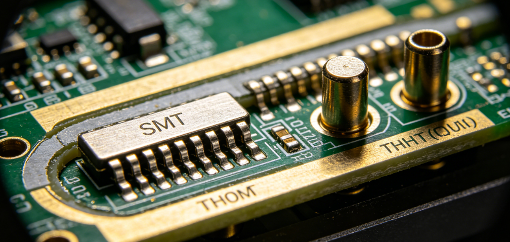
Leveraging Blind and Buried Vias in PCB Design
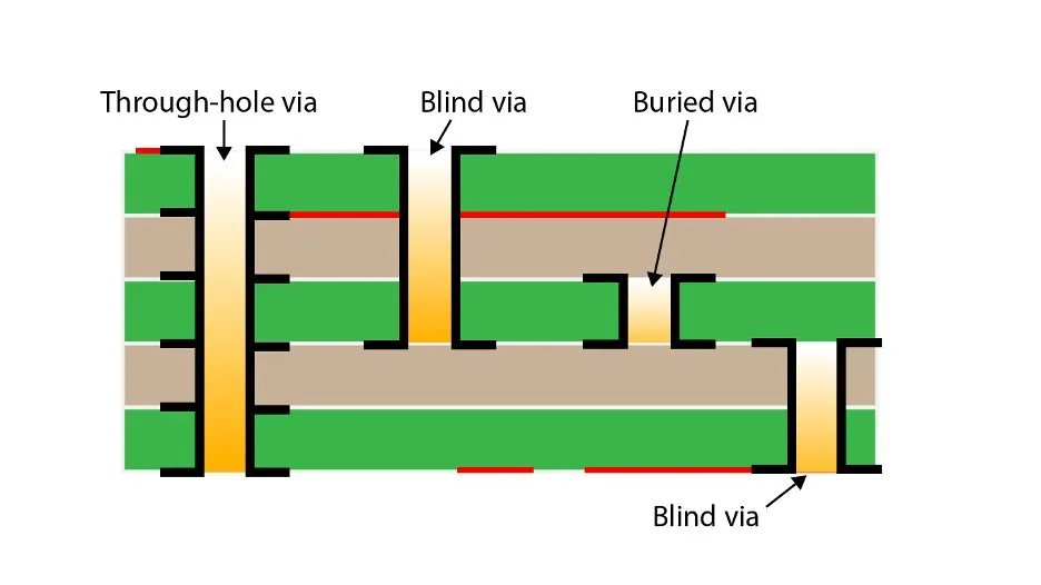
Vias are small holes in a PCB that connect different layers, but not all vias span the entire board. Blind and buried vias in PCB design are advanced techniques used to save space and improve routing efficiency, especially in high-density layouts.
Blind Vias connect an outer layer to an inner layer without passing through the entire board. For example, in a 4-layer PCB, a blind via might connect the top layer to the second layer, leaving the bottom layers free for other connections. This is particularly useful in designs where surface space is limited due to dense component placement.
Buried Vias, on the other hand, connect internal layers without reaching the outer surfaces. These are ideal for multi-layer boards with 6 or more layers, as they allow internal routing without occupying valuable surface real estate. However, they increase manufacturing complexity and cost, often adding 20-30% to production expenses compared to standard through-hole vias.
Using blind and buried vias can reduce board size by up to 15% in high-density interconnect (HDI) designs, making them a go-to choice for compact devices like smartphones and wearables. When implementing these vias, ensure proper aspect ratios (via depth to diameter) are maintained—typically below 1:1 for blind vias—to avoid fabrication issues.
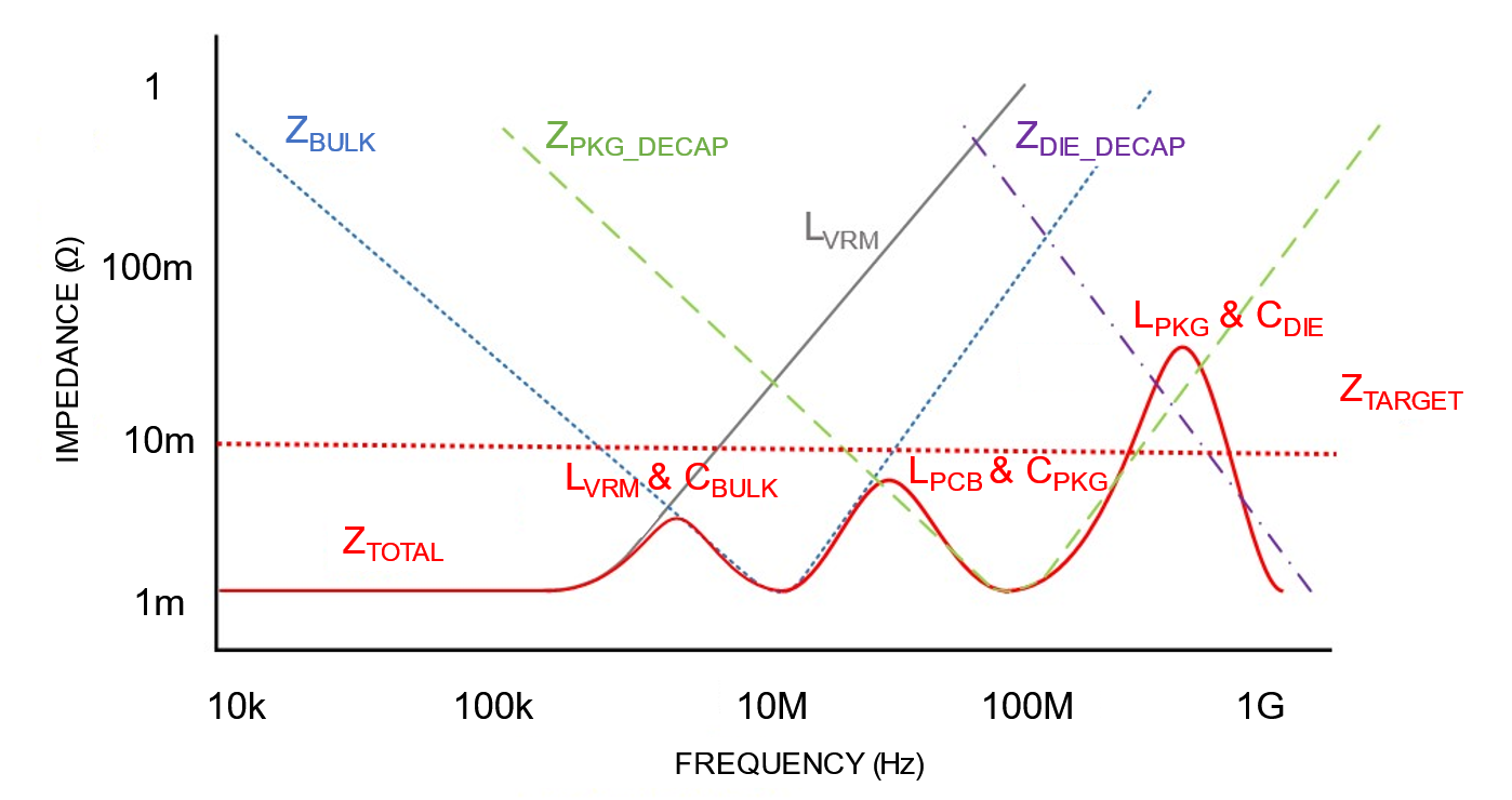
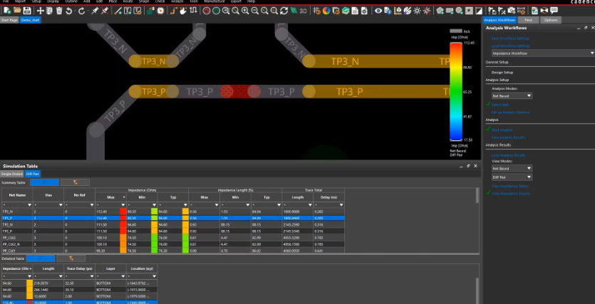
Mastering Impedance Control Routing for Signal Integrity
In high-speed PCB designs, maintaining signal integrity is paramount, and impedance control routing is a key technique to achieve this. Impedance, measured in ohms, refers to the resistance a signal encounters as it travels along a trace. Mismatched impedance can cause signal reflections, leading to data loss or errors in systems operating at speeds above 1 GHz.
To control impedance, designers must consider trace width, trace spacing, and the dielectric properties of the PCB material. For instance, a 50-ohm impedance is standard for many high-speed applications like USB or Ethernet. Using a trace width of 5 mils on a standard FR-4 material with a dielectric thickness of 10 mils can achieve this target impedance, though calculations using impedance calculators or simulation software are recommended for precision.
Here are some tips for effective impedance control routing:
- Consistent Trace Geometry: Keep trace widths and spacing uniform to avoid impedance discontinuities.
- Reference Planes: Route high-speed signals over a continuous ground plane to provide a stable return path.
- Layer Stackup: Position high-speed traces on layers adjacent to a ground plane to minimize signal distortion.
By prioritizing impedance control, you can reduce signal degradation by up to 40% in high-frequency designs, ensuring reliable performance in critical applications.
Differential Pair Routing Techniques for High-Speed Signals
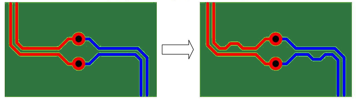
High-speed digital signals often use differential pairs—two traces carrying complementary signals—to improve noise immunity and signal integrity. Differential pair routing techniques are essential for designs involving interfaces like USB, HDMI, or PCIe, where data rates can exceed 5 Gbps.
The key to successful differential pair routing is maintaining symmetry between the two traces. Any mismatch in length or spacing can introduce skew, leading to timing errors. For example, in a USB 3.0 design, the length difference between the pair should be less than 5 mils to keep skew under 15 picoseconds.
Follow these best practices for differential pair routing:
- Equal Lengths: Match the lengths of the two traces as closely as possible using serpentine routing if necessary.
- Consistent Spacing: Maintain a fixed gap (typically 3-5 times the trace width) between the traces to ensure consistent coupling.
- Avoid Sharp Bends: Use 45-degree angles or smooth curves instead of 90-degree turns to minimize signal reflections.
Proper differential pair routing can reduce electromagnetic interference by up to 30%, making it a critical technique for high-speed PCB designs.
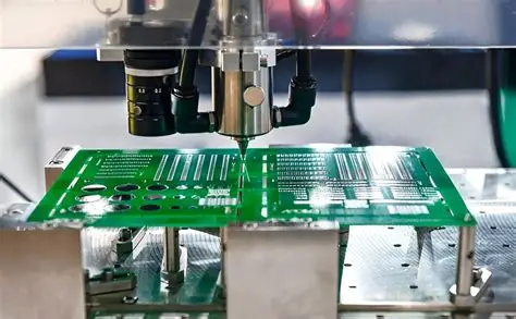
High-Density Interconnect PCB Routing for Compact Designs
As electronic devices become smaller and more powerful, high-density interconnect PCB routing (HDI) has emerged as a vital technique for fitting more functionality into limited space. HDI designs use finer traces, smaller vias, and higher layer counts to achieve greater component density.
In HDI routing, trace widths can be as narrow as 3 mils, and microvias (vias with diameters below 6 mils) are often used to connect layers. This allows for routing under surface-mounted components, maximizing board space. For instance, in a modern smartphone PCB, HDI techniques can support over 100 components per square inch, a feat impossible with traditional routing methods.
Key considerations for HDI routing include:
- Microvias: Use laser-drilled microvias for connections in tight spaces, ensuring aspect ratios below 0.75:1 for reliability.
- Fine-Pitch Components: Route traces for fine-pitch components (e.g., 0.4 mm BGA) with precision to avoid short circuits.
- Layer Planning: Allocate specific layers for power distribution and signal routing to minimize interference in dense areas.
HDI routing can increase component density by 25-40%, making it ideal for compact, high-performance devices. However, it requires advanced manufacturing capabilities and careful design to avoid signal integrity issues.
Practical Tips for Implementing Advanced PCB Routing Techniques
Now that we’ve covered the core concepts, here are some actionable tips to integrate these advanced techniques into your PCB designs:
- Simulation Tools: Use simulation software to model impedance, signal integrity, and EMI before finalizing your layout. This can save up to 20% in rework costs by catching issues early.
- Design Rules: Set strict design rules for trace widths, via sizes, and spacing based on your project’s requirements to ensure consistency.
- Collaboration: Work closely with your manufacturing partner to confirm that your design aligns with their capabilities, especially for HDI or blind/buried vias.
- Thermal Management: Incorporate thermal vias and heat sinks in multi-layer designs to manage heat dissipation, especially in power-heavy applications.
By combining these practices with the techniques discussed, you can create robust PCB designs that meet the demands of modern electronics.
Conclusion: Elevating Your PCB Design Skills
Mastering advanced PCB routing techniques is a game-changer for engineers and designers working on multi-layer boards. From optimizing multi-layer PCB stackup design to implementing blind and buried vias in PCB, controlling impedance, perfecting differential pair routing techniques, and embracing high-density interconnect PCB routing, each method contributes to building more reliable and efficient circuits.
These strategies not only improve signal integrity and performance but also enable the creation of compact, cutting-edge devices. As technology continues to push boundaries, staying ahead with these advanced techniques will ensure your designs stand out in a competitive field. Start applying these insights to your next project and witness the difference in quality and efficiency.