ALLPCB


In the world of electronics, designing printed circuit boards (PCBs) for high-speed digital circuits is both a challenge and a necessity. As devices become faster and more complex, ensuring signal integrity, controlling impedance, and minimizing crosstalk are critical for performance. If you're looking for advanced PCB layout techniques to master high-speed design, you're in the right place. This guide dives deep into high-speed PCB design rules, signal integrity PCB layout strategies, impedance control methods, differential pair routing guides, and crosstalk minimization techniques to help you create reliable and efficient boards.
Whether you're an experienced engineer or just stepping into high-speed design, this comprehensive blog will walk you through actionable tips and best practices. Let's explore how to optimize your PCB layouts for the demands of modern digital circuits.
Why High-Speed PCB Design Matters
High-speed digital circuits operate at frequencies where even small design flaws can lead to significant issues like signal distortion, data loss, or electromagnetic interference (EMI). With clock speeds often exceeding 100 MHz and edge rates in the nanosecond range, traditional PCB design approaches fall short. High-speed PCB design rules are essential to maintain signal integrity and ensure that your circuit performs as intended.
The stakes are high in applications like telecommunications, data centers, and automotive electronics. A poorly designed PCB can result in timing errors, increased noise, or complete system failure. By following advanced layout techniques, you can mitigate these risks and build boards that support faster data rates and reliable operation.
Key Principles of High-Speed PCB Design Rules
Before diving into specific techniques, let's cover the foundational principles that guide high-speed PCB design. These rules form the backbone of any successful layout and address the core challenges of signal integrity and performance.
- Minimize Signal Path Lengths: Shorter traces reduce signal delay and lower the risk of interference. For high-speed signals above 100 MHz, aim to keep trace lengths under 1 inch where possible.
- Control Impedance: Impedance mismatches can cause signal reflections, leading to data corruption. Target a specific impedance value, such as 50 ohms for single-ended traces or 100 ohms for differential pairs, based on your design requirements.
- Use Proper Grounding: A solid ground plane is crucial for reducing noise and providing a return path for high-speed signals. Avoid splitting ground planes under critical signal traces.
- Avoid Sharp Corners: Use 45-degree angles or curved traces instead of 90-degree corners to prevent signal reflections and EMI.
These rules set the stage for more advanced techniques. Let's explore specific strategies for optimizing your PCB layout.
Signal Integrity PCB Layout: Ensuring Clean Data Transmission
Signal integrity (SI) refers to the quality of an electrical signal as it travels through a PCB. Poor SI can lead to timing errors, jitter, or data loss, especially in high-speed digital circuits. Here are key practices for maintaining signal integrity in your PCB layout:
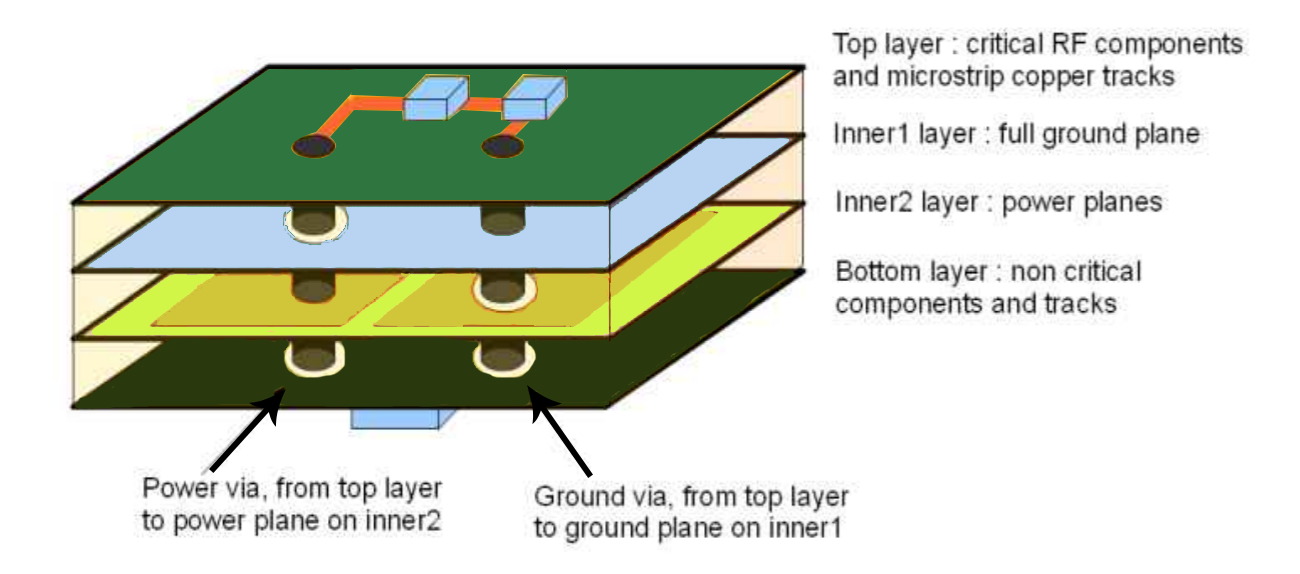
1. Layer Stackup Design
A well-planned layer stackup is the foundation of signal integrity. Place high-speed signal traces on layers adjacent to a continuous ground plane to provide a low-impedance return path. For a 4-layer board, a common stackup might be:
- Top Layer: Signal traces
- Layer 2: Ground plane
- Layer 3: Power plane
- Bottom Layer: Signal traces
This configuration minimizes noise and ensures a consistent reference for high-speed signals.
2. Trace Width and Spacing
Trace width affects impedance, while spacing impacts crosstalk. Use a PCB design tool to calculate the appropriate width for a target impedance (e.g., 50 ohms). Maintain at least 3 times the trace width as spacing between adjacent high-speed traces to reduce interference.
3. Via Management
Vias introduce inductance and capacitance, which can degrade signal integrity. Minimize the number of vias on high-speed traces, and use back-drilling for through-hole vias to remove unused stubs that cause reflections.
Impedance Control PCB: Matching for Optimal Performance
Impedance control is a critical aspect of high-speed PCB design. Mismatched impedance between a source, trace, and load causes signal reflections, which can corrupt data. Here's how to achieve proper impedance control in your PCB layout:
1. Calculate Target Impedance
Determine the required impedance for your traces based on the components and standards you're using. For example, USB 2.0 requires a differential impedance of 90 ohms, while Ethernet often uses 100 ohms. Use an impedance calculator or simulation tool to define trace width, dielectric thickness, and material properties.
2. Use Consistent Materials
The dielectric constant (Dk) of your PCB material affects impedance. Standard FR-4 material has a Dk of around 4.2-4.5, but for high-speed designs, consider low-loss materials like Rogers or Isola with a Dk closer to 3.0-3.5 for better control.
3. Terminate Signals Properly
Add termination resistors near the receiver to match the trace impedance and prevent reflections. For a 50-ohm trace, use a 50-ohm resistor in series or parallel, depending on the circuit requirements.
By maintaining consistent impedance across your PCB, you ensure that signals arrive at their destination without distortion or loss.
Differential Pair Routing Guide: Precision for High-Speed Signals
Differential pairs are commonly used in high-speed designs like USB, HDMI, and Ethernet to transmit data with high noise immunity. However, improper routing can lead to signal skew and EMI. Follow this differential pair routing guide for optimal results:
1. Match Lengths Precisely
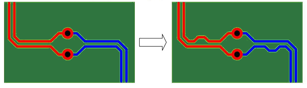
Ensure that both traces in a differential pair are of equal length to avoid timing skew. A mismatch of even 10 mils (0.010 inches) can cause significant issues at frequencies above 1 GHz. Use serpentine routing to lengthen the shorter trace if needed.
2. Maintain Consistent Spacing
Keep the spacing between the two traces constant to maintain the target differential impedance (e.g., 100 ohms). A common rule is to keep the spacing less than or equal to the trace width.
3. Avoid Crossing Splits
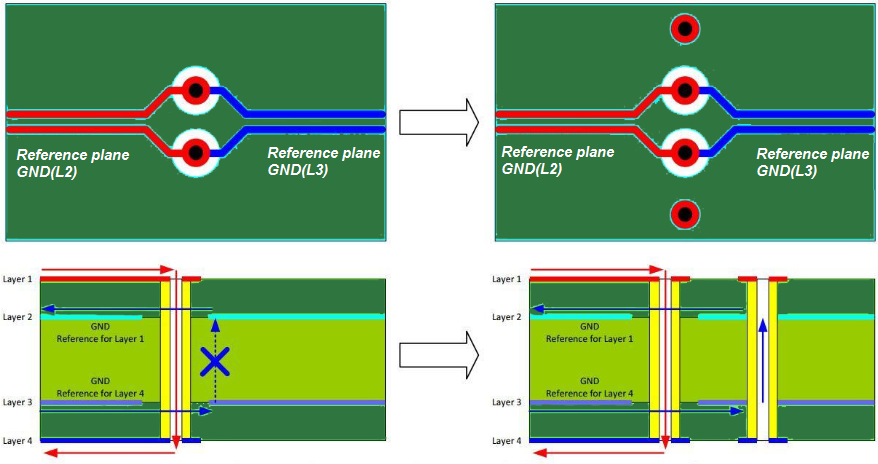
Do not route differential pairs over splits in the ground or power planes, as this disrupts the return path and introduces noise. If crossing a split is unavoidable, add a stitching capacitor near the split to provide a return path.
Crosstalk Minimization Techniques: Reducing Interference
Crosstalk occurs when signals on adjacent traces interfere with each other, causing noise and data errors. In high-speed designs, where edge rates are fast (e.g., below 1 ns), crosstalk becomes a major concern. Use these crosstalk minimization techniques to keep your signals clean:
1. Increase Trace Spacing
The closer traces are, the stronger the electromagnetic coupling. Maintain a spacing of at least 3 times the trace width between high-speed signals. For critical signals, increase this to 5 times the width if space allows.
2. Use Ground Planes Effectively
A continuous ground plane beneath signal traces acts as a shield, reducing crosstalk. Ensure that the ground plane is unbroken under high-speed traces to provide a low-impedance return path.
3. Route Signals on Different Layers
If spacing is limited, route high-speed signals on separate layers with a ground plane between them. This physical separation significantly reduces coupling and interference.
4. Control Signal Edge Rates
Faster edge rates increase crosstalk. If possible, use components with slower rise and fall times for non-critical signals to reduce coupling to adjacent traces.
By applying these techniques, you can minimize crosstalk and ensure that your high-speed signals remain clear and reliable.
Additional Tips for High-Speed PCB Layout Success
Beyond the core techniques discussed, here are a few additional strategies to enhance your high-speed PCB design:
- Simulate Before Building: Use simulation tools to model signal integrity, impedance, and crosstalk before manufacturing. This can save time and cost by identifying issues early.
- Decouple Power Supplies: Place decoupling capacitors (e.g., 0.1 μF and 1 μF) close to IC power pins to reduce noise on the power plane, which can affect high-speed signals.
- Optimize Component Placement: Position high-speed components close to each other to minimize trace lengths and reduce the risk of interference.
Common Pitfalls to Avoid in High-Speed PCB Design
Even with the best techniques, mistakes can happen. Here are common pitfalls to watch out for:
- Ignoring Return Paths: High-speed signals need a continuous return path. Avoid routing over splits in ground planes without proper stitching.
- Overusing Vias: Excessive vias on high-speed traces introduce inductance and degrade signal quality. Keep via count to a minimum.
- Neglecting EMI: High-speed circuits are prone to emitting EMI. Use shielding, proper grounding, and filtering to keep emissions in check.
Being aware of these issues can help you design more robust and reliable PCBs for high-speed applications.
Conclusion: Mastering High-Speed PCB Layout
Designing PCBs for high-speed digital circuits requires precision, planning, and adherence to best practices. By following advanced PCB layout techniques—such as maintaining signal integrity, controlling impedance, routing differential pairs correctly, and minimizing crosstalk—you can create boards that perform reliably even at the highest frequencies.
Start with a solid foundation of high-speed PCB design rules, and build on it with strategies like proper layer stackup, precise impedance matching, and effective grounding. Use simulation tools to validate your design, and always prioritize signal quality over convenience. With these principles in mind, you're well-equipped to tackle the challenges of modern electronics design.
At ALLPCB, we’re committed to supporting engineers with resources and expertise for high-speed PCB projects. Whether you're working on a data-intensive application or a cutting-edge device, applying these techniques will help you achieve success in your designs.