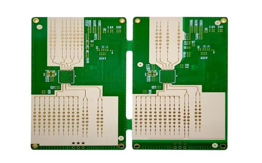
Are you looking to design a printed circuit board (PCB) for blockchain mining without breaking the bank? Open source PCB design software offers a powerful, cost-effective solution for creating high-performance mining hardware. In this comprehensive guide, we’ll explore how to use open source tools like KiCad for mining PCB design, dive into FreePCB alternatives, and highlight the benefits of community support for open source EDA tools, along with significant cost savings with open source PCB tools. Whether you're a hobbyist or a professional engineer, this blog will walk you through the essentials of designing PCBs tailored for blockchain mining using free and accessible resources.
Why Use Open Source Tools for Blockchain Mining PCB Design?
Blockchain mining, especially for cryptocurrencies like Bitcoin, requires specialized hardware such as ASICs (Application-Specific Integrated Circuits) or GPUs. Designing PCBs for these mining rigs demands precision, efficiency, and often, tight budgets. Open source PCB design software provides a viable path to achieve professional-grade designs without the hefty price tag of proprietary tools. These tools are not only free but also backed by active communities that offer support, plugins, and regular updates.
By leveraging open source EDA (Electronic Design Automation) tools, you can save thousands of dollars on licensing fees while still accessing advanced features like schematic capture, PCB layout, and 3D visualization. Let’s dive deeper into how these tools can be applied specifically to mining hardware and what benefits they bring to the table.
Understanding Blockchain Mining PCB Requirements
Before jumping into software, it’s crucial to understand the unique demands of blockchain mining PCBs. Mining hardware operates under high stress, with constant power draw and heat generation. Here are some key considerations for designing such PCBs:
- Power Delivery: Mining rigs require robust power distribution networks to handle high currents, often exceeding 100A for ASIC-based designs. This means wide traces (e.g., 50-100 mils for high-current paths) and multiple power planes to minimize voltage drops.
- Thermal Management: Heat dissipation is critical. PCBs must include thermal vias and copper pours to transfer heat away from components, maintaining temperatures below 85°C for optimal performance.
- Signal Integrity: High-speed data lines between mining chips and controllers must maintain signal integrity, often requiring controlled impedance traces (e.g., 50 ohms for differential pairs) and minimal crosstalk.
- Compact Layouts: Mining hardware often packs many components into tight spaces, necessitating efficient use of board real estate while avoiding interference.
With these requirements in mind, open source tools can help you design PCBs that meet these stringent needs without compromising on quality.
Top Open Source PCB Design Software for Mining Projects
Let’s explore some of the best open source PCB design software options available for blockchain mining projects. These tools are chosen for their capabilities, ease of use, and strong community support.
KiCad for Mining PCB Design
KiCad is arguably the most popular open source EDA tool available today. It offers a complete suite for schematic capture, PCB layout, and 3D rendering, making it an excellent choice for designing mining hardware. Available on Windows, macOS, and Linux, KiCad is forever free with no limitations on board size or layer count.
For blockchain mining PCBs, KiCad shines with features like:
- Advanced Routing: KiCad supports interactive routing and differential pair routing, essential for maintaining signal integrity on high-speed mining boards.
- Thermal Analysis Tools: Plugins and built-in features allow you to simulate heat distribution and place thermal vias effectively.
- Extensive Libraries: Access to vast component libraries means you can find or create footprints for mining-specific chips and connectors.
KiCad also benefits from a vibrant user base that contributes plugins and tutorials. For instance, you can use third-party tools to calculate trace widths for high-current paths (e.g., a 100-mil trace for 10A at 1 oz copper thickness) directly within the software.
FreePCB Alternatives for Blockchain Mining
While FreePCB was once a go-to open source tool for PCB design, it has become outdated with limited updates and support. Fortunately, several FreePCB alternatives offer modern features and active development, making them better suited for complex mining designs.
- LibrePCB: A newer open source tool, LibrePCB focuses on user-friendliness and cross-platform compatibility. It’s ideal for simpler mining PCB projects with its intuitive interface and integrated library management. While it lacks some advanced features of KiCad, it’s a good starting point for beginners.
- Fritzing: Though primarily aimed at hobbyists, Fritzing can be useful for prototyping mining control boards. It offers a breadboard view alongside schematic and PCB layouts, making it easier to visualize connections. However, it’s less suited for high-density or high-power designs due to limited routing capabilities.
These alternatives provide flexibility depending on your project’s complexity. For high-performance mining rigs, KiCad remains the top choice due to its robustness and scalability.
Community Support for Open Source EDA Tools
One of the standout advantages of using open source PCB design software is the community support for open source EDA tools. Unlike proprietary software where support often comes at a premium, open source communities are filled with passionate engineers and hobbyists eager to help.
For KiCad, the community is particularly strong. Online forums, social media groups, and dedicated websites offer a wealth of resources:
- Tutorials and Guides: Step-by-step guides on designing high-current PCBs or optimizing layouts for thermal performance are widely available.
- Plugins and Add-ons: Community-developed plugins enhance KiCad’s functionality, such as tools for calculating trace impedance or automating repetitive tasks.
- Feedback and Troubleshooting: If you encounter issues like signal noise in your mining PCB (e.g., crosstalk on a 3.3V data line), community members often provide quick solutions based on real-world experience.
This collaborative environment ensures that even complex challenges in blockchain mining PCB design can be addressed without costly support contracts.
Cost Savings with Open Source PCB Tools
Perhaps the most compelling reason to adopt open source tools is the cost savings with open source PCB tools. Traditional EDA software can cost anywhere from $1,000 to $10,000 per year in licensing fees, a significant barrier for startups, small businesses, or individual engineers working on mining hardware.
With open source software like KiCad, you get:
- Zero Licensing Costs: No upfront fees or recurring subscriptions mean you can allocate your budget to hardware components or prototyping.
- No Feature Limitations: Unlike free versions of commercial software, open source tools don’t lock advanced features behind paywalls. You can design multi-layer boards (e.g., 6-layer PCBs for mining rigs) without additional costs.
- Scalability: Whether you’re designing a single board or managing a large project, the software remains free regardless of scale.
For a small mining hardware startup, switching to open source tools could save upwards of $5,000 annually on software alone. These savings can be reinvested into better components or faster prototyping cycles, giving you a competitive edge.
Step-by-Step Guide to Designing a Mining PCB with KiCad
Now that we’ve covered the benefits, let’s walk through a practical example of designing a simple mining PCB using KiCad. This guide focuses on a basic control board for a mining rig, but the principles apply to more complex designs.
- Install KiCad: Download and install KiCad from its official website. It’s compatible with most operating systems and regularly updated.
- Create a New Project: Start a new project and set up your schematic editor. Define the basic components like power regulators, mining chip interfaces, and connectors.
- Design the Schematic: Use KiCad’s library to add components. For a mining board, include high-current MOSFETs for power switching and ensure proper voltage ratings (e.g., 12V input for ASIC miners).
- Assign Footprints: Link each schematic symbol to a physical footprint. Double-check that footprints match your components’ dimensions to avoid manufacturing errors.
- Layout the PCB: Switch to the PCB editor and arrange components to minimize trace lengths for high-speed signals. Use wider traces (e.g., 80 mils) for power lines to handle currents up to 15A.
- Add Thermal Management: Place thermal vias under heat-generating components and use copper pours for heat dissipation. KiCad’s 3D viewer helps visualize heat paths.
- Validate and Export: Run design rule checks (DRC) to ensure no errors, then export Gerber files for manufacturing.
This process leverages KiCad’s full capabilities to create a mining PCB optimized for performance and reliability, all at no software cost.
Challenges and Solutions in Open Source PCB Design for Mining
While open source tools are powerful, they’re not without challenges, especially for specialized applications like blockchain mining. Here are some common hurdles and how to overcome them:
- Learning Curve: Tools like KiCad can be intimidating for beginners due to their extensive features. Solution: Use online tutorials and community resources to get up to speed. Start with smaller projects before tackling complex mining boards.
- Limited Advanced Simulation: Unlike some commercial tools, open source software may lack built-in power integrity or electromagnetic simulation. Solution: Integrate third-party tools or plugins for simulation, or rely on community-shared scripts for analysis.
- Component Library Gaps: You might not find footprints for the latest mining chips. Solution: Create custom footprints using KiCad’s editor or download them from community-shared libraries.
By addressing these challenges head-on, you can fully harness the potential of open source tools for your mining projects.
Conclusion: Empowering Mining Innovation with Open Source Tools
Designing PCBs for blockchain mining doesn’t have to come with a high price tag. Open source PCB design software like KiCad offers a robust, free alternative to expensive proprietary tools, delivering features tailored to the unique demands of mining hardware. With strong community support for open source EDA tools and significant cost savings with open source PCB tools, engineers and hobbyists alike can innovate without financial barriers.
Whether you’re exploring KiCad for mining PCB design or seeking FreePCB alternatives, the open source ecosystem provides the flexibility and resources to bring your mining hardware ideas to life. Start experimenting with these tools today, and take advantage of the collaborative spirit of the open source community to optimize your designs for power, heat, and efficiency.
At ALLPCB, we’re committed to supporting your PCB design journey, from concept to production. With the right open source tools in hand, you’re well-equipped to tackle the challenges of blockchain mining hardware and drive the future of cryptocurrency technology.
 ALLPCB


