 ALLPCB


In today’s fast-paced world of electronics, smaller, faster, and more efficient devices are the name of the game. If you’re wondering how to achieve compact designs without sacrificing performance, High-Density Interconnect (HDI) PCB technology is the answer. This innovative approach allows for significant size reduction while boosting functionality, making it a go-to solution for modern electronics. In this blog, we’ll explore HDI PCB miniaturization benefits, dive into high-density interconnect PCB applications, and uncover HDI PCB size reduction techniques to help engineers and designers unlock the full potential of their projects.
Whether you’re working on cutting-edge consumer gadgets or complex industrial systems, understanding HDI technology can transform your designs. Let’s take a deep dive into what makes HDI PCBs a game-changer and how you can leverage them for your next innovation.
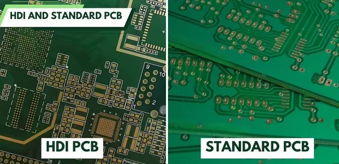
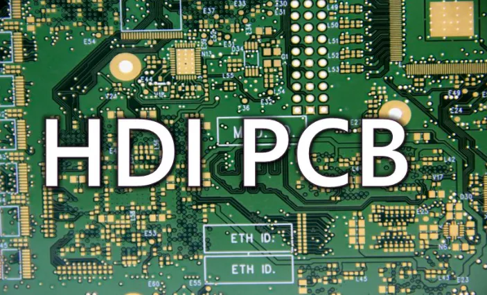
What is HDI PCB Technology?
High-Density Interconnect (HDI) PCB technology refers to printed circuit boards with a higher wiring density per unit area compared to traditional PCBs. This is achieved through finer lines and spaces, smaller vias (often microvias), and higher connection pad density. As defined by industry standards like IPC-2226, HDI PCBs are designed to pack more components into a smaller footprint, making them ideal for compact and high-performance electronics.
The core idea behind HDI is to optimize space while maintaining or even improving signal integrity and performance. By using advanced manufacturing techniques like laser drilling for microvias and thinner materials, HDI PCBs enable engineers to create smaller, lighter, and more powerful devices.
The Benefits of HDI PCB Miniaturization
One of the standout advantages of HDI technology is its ability to shrink the size of electronic devices without compromising on functionality. Let’s break down the key HDI PCB miniaturization benefits that make it a top choice for engineers:
- Significant Size Reduction: HDI PCBs can reduce board size by up to 60%, as noted in recent industry insights. This is critical for applications like smartphones, wearables, and medical devices where space is at a premium.
- Increased Component Density: With finer traces (often below 75 micrometers) and smaller vias (as small as 0.1 mm), HDI boards can accommodate more components in a smaller area, allowing for complex designs in compact spaces.
- Improved Signal Integrity: Shorter interconnects in HDI designs reduce signal loss and crosstalk, ensuring faster data transmission. For high-speed applications, this can mean maintaining signal integrity at frequencies above 1 GHz.
- Reduced Weight: Smaller boards with thinner materials lead to lighter devices, which is a huge advantage in industries like aerospace and automotive where every gram counts.
- Cost Efficiency in the Long Run: While HDI manufacturing can have higher upfront costs, the reduced board size and layer count often lower material expenses and improve yield over time.
These benefits collectively enable the creation of next-generation devices that are not only smaller but also more reliable and efficient, meeting the demands of modern technology.
High-Density Interconnect PCB Applications
The versatility of HDI technology makes it a perfect fit for a wide range of industries. Below, we explore some of the most prominent high-density interconnect PCB applications where this technology shines:
1. Consumer Electronics
From smartphones to smartwatches, consumer electronics rely heavily on HDI PCBs to pack powerful features into tiny devices. For instance, modern smartphones often use HDI boards with 6-10 layers to integrate processors, cameras, and sensors into a slim form factor.
2. Medical Devices
In the medical field, HDI technology is used in compact diagnostic equipment, wearable health monitors, and implantable devices. The small size and high reliability of HDI PCBs ensure that life-saving tools like pacemakers or glucose monitors function flawlessly in constrained spaces.
3. Automotive Systems
With the rise of electric vehicles and advanced driver-assistance systems (ADAS), automotive electronics require robust and compact solutions. HDI PCBs are used in control units, sensors, and infotainment systems, supporting high-speed data transfer and durability under harsh conditions.
4. Telecommunications
The rollout of 5G technology has increased the demand for HDI PCBs in base stations, routers, and other networking equipment. These boards handle high-frequency signals (up to 28 GHz in some 5G applications) while maintaining a small footprint.
5. Aerospace and Defense
In aerospace and defense, where reliability and weight reduction are critical, HDI PCBs are used in navigation systems, radar equipment, and satellite components. Their ability to withstand extreme environments while minimizing size is invaluable.
HDI PCB Size Reduction Techniques
Achieving miniaturization with HDI technology involves a combination of advanced design and manufacturing strategies. Here are the most effective HDI PCB size reduction techniques that engineers can apply to optimize their designs:
1. Use of Microvias
Microvias, typically with diameters of 0.1 mm or less, are a cornerstone of HDI design. Unlike traditional through-hole vias, microvias are created using laser drilling and connect only specific layers, saving space and allowing for denser routing. This technique can increase connection density by up to 50% compared to standard vias.
2. Fine Line and Space Technology
HDI PCBs often feature trace widths and spacing as narrow as 50-75 micrometers. This precision, achieved through advanced photolithography, allows more circuits to fit into a smaller area, reducing the overall board size without sacrificing functionality.
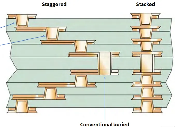
3. Stacked and Staggered Via Structures
Stacked vias (vias placed directly on top of each other) and staggered vias (offset vias) help connect multiple layers in a compact manner. These structures minimize the space needed for interconnections, enabling multi-layer HDI boards with up to 12 or more layers in a thin profile.
4. Thin Dielectric Materials
Using ultra-thin dielectric layers, often less than 0.1 mm thick, reduces the overall thickness of the PCB. Materials like polyimide or advanced FR-4 variants provide the necessary insulation while supporting high-density designs, contributing to a slimmer board.
5. Build-Up Layer Technology
HDI PCBs often use a sequential build-up (SBU) process, where layers are added one at a time with microvias connecting them. This method allows for precise control over layer count and thickness, optimizing space compared to traditional laminated multilayer boards.
6. Embedded Components
Embedding passive components like resistors and capacitors directly into the PCB substrate frees up surface space for active components. This technique can reduce board size by up to 30% in some designs, especially for high-density applications.
Design Considerations for HDI PCBs
While HDI technology offers incredible benefits, it also comes with unique design challenges. Here are some key considerations to keep in mind when working with HDI PCBs to ensure optimal performance and manufacturability:
- Thermal Management: High component density can lead to heat buildup. Incorporate thermal vias and heat sinks to dissipate heat effectively, especially in high-power applications.
- Signal Integrity: At high frequencies, impedance mismatches can degrade performance. Maintain consistent trace widths and use simulation tools to ensure controlled impedance, often targeting values like 50 ohms for RF applications.
- Manufacturing Constraints: Work closely with your PCB fabrication partner to understand their capabilities for microvia drilling, line spacing, and material options. Typical aspect ratios for microvias should not exceed 0.75:1 for reliable plating.
- Cost vs. Performance: Balance the complexity of your HDI design with budget constraints. Adding more layers or finer features increases costs, so prioritize critical areas for high-density routing.
By addressing these factors during the design phase, you can avoid common pitfalls and maximize the advantages of HDI technology.
Challenges in HDI PCB Manufacturing
While HDI PCBs offer unparalleled benefits, their manufacturing process is more complex than that of traditional boards. Some challenges include:
- Higher Precision Requirements: Laser drilling for microvias and fine line etching demand advanced equipment and tight tolerances, often within ±10 micrometers.
- Material Selection: Thin dielectrics and high-performance laminates must withstand thermal and mechanical stress during fabrication and operation.
- Increased Testing Needs: With denser layouts, thorough testing for shorts, opens, and signal integrity is essential to ensure reliability.
Partnering with an experienced PCB manufacturer can help overcome these hurdles by leveraging cutting-edge technology and expertise in HDI production.
Future Trends in HDI PCB Technology
As technology continues to evolve, HDI PCBs are poised to play an even bigger role in shaping the future of electronics. Some emerging trends include:
- Ultra-HDI Designs: Pushing the limits of miniaturization with line widths below 30 micrometers for next-gen devices.
- Integration with Flexible PCBs: Combining HDI with flexible substrates for wearable and foldable electronics.
- AI and IoT Applications: Supporting the massive connectivity demands of smart devices with compact, high-speed HDI boards.
Staying ahead of these trends can give engineers a competitive edge in designing innovative products for tomorrow’s challenges.
Conclusion: Why HDI PCB Technology is the Key to Miniaturization
HDI PCB technology is revolutionizing the electronics industry by enabling smaller, faster, and more efficient devices. With significant HDI PCB miniaturization benefits like size reduction and improved signal integrity, a wide range of high-density interconnect PCB applications across industries, and proven HDI PCB size reduction techniques like microvias and fine line technology, HDI is the foundation of modern design innovation.
For engineers and designers looking to push the boundaries of what’s possible, embracing HDI technology offers a clear path to creating cutting-edge solutions. By understanding its advantages, applications, and design strategies, you can unlock the full potential of miniaturization for your next project. Let HDI PCBs be the key to transforming your ideas into reality with unmatched performance and efficiency.


