Designing printed circuit boards (PCBs) for navigation systems is a challenging task. These systems, used in automotive, aerospace, marine, and personal devices, rely on precision and reliability to ensure accurate positioning and communication. However, issues like signal integrity problems, power distribution failures, and impedance mismatches can disrupt performance. In this comprehensive guide, we’ll dive into troubleshooting common issues in navigation system PCB design, focusing on practical solutions for navigation PCB debugging, navigation PCB error detection, navigation PCB signal integrity issues, navigation PCB power distribution problems, and navigation PCB impedance mismatch. Let’s explore how to identify and fix these problems to create robust and reliable designs.
Why Navigation System PCBs Are Prone to Issues
Navigation systems often operate in harsh environments with high-frequency signals, tight timing requirements, and strict power constraints. Whether it’s a GPS module in a car or a satellite communication system in an aircraft, the PCB must handle complex data processing while maintaining accuracy. Common challenges include interference from nearby electronics, temperature fluctuations, and the need for compact layouts. Understanding these factors is the first step in effective navigation PCB debugging and error prevention.
Common Issues in Navigation System PCB Design
Let’s break down the most frequent problems encountered during the design and operation of navigation system PCBs. Each section will cover identification, causes, and actionable solutions.
1. Navigation PCB Signal Integrity Issues
Signal integrity is critical in navigation systems, where high-frequency signals from GPS, GNSS, or other communication protocols are processed. Navigation PCB signal integrity issues can lead to data loss, timing errors, or complete system failure. Common symptoms include jitter, crosstalk, and signal reflections.
Causes:
- Poor Trace Routing: Long or improperly routed traces can introduce delays or interference. For example, a trace running parallel to another high-speed line might cause crosstalk.
- Inadequate Ground Planes: A broken or poorly designed ground plane can disrupt the return path of high-frequency signals, leading to noise.
- Component Placement: Placing sensitive components like RF receivers near noisy elements can degrade signal quality.
Solutions for Navigation PCB Signal Integrity Issues:
- Optimize Trace Lengths: Keep high-speed traces as short as possible. For GPS signals operating at 1.575 GHz, even a few millimeters of extra length can introduce significant delay.
- Use Continuous Ground Planes: Ensure a solid ground plane beneath signal layers to provide a low-impedance return path. Avoid splitting the ground plane unless absolutely necessary.
- Shield Sensitive Areas: Use guard traces or shielding around RF components to minimize interference.
- Simulation Tools: Leverage simulation software to analyze signal behavior before fabrication. This can help predict and mitigate potential issues.
2. Navigation PCB Power Distribution Problems
Power distribution is another common hurdle in navigation PCB design. Navigation PCB power distribution problems can cause voltage drops, noise in the power supply, or insufficient current to critical components like microcontrollers or RF modules.
Causes:
- Inadequate Decoupling Capacitors: Without proper decoupling, high-frequency noise from switching components can affect sensitive circuits.
- Poor Power Plane Design: Narrow traces or insufficient copper thickness can lead to voltage drops, especially in high-current areas.
- Thermal Issues: Overheating in power delivery components can reduce efficiency and cause failures.
Solutions for Navigation PCB Power Distribution Problems:
- Place Decoupling Capacitors Strategically: Position capacitors close to power pins of ICs. For instance, a 0.1 μF capacitor near a GPS chipset can filter out noise effectively.
- Design Robust Power Planes: Use wide traces or dedicated power planes to ensure low resistance. A typical navigation system might require a 3.3V supply with minimal drop, so aim for traces that can handle at least 1A of current without significant loss.
- Thermal Management: Add heat sinks or thermal vias near power regulators to dissipate heat. Ensure the PCB material can handle temperatures up to 85°C, common in automotive navigation environments.
3. Navigation PCB Impedance Mismatch
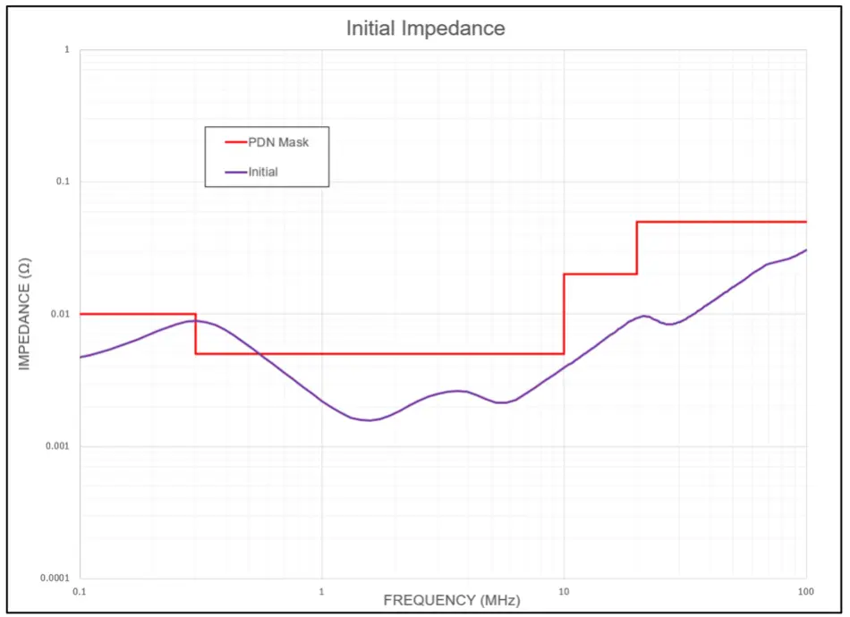
Impedance mismatch is a frequent issue in high-frequency designs like navigation systems. Navigation PCB impedance mismatch occurs when the impedance of traces, connectors, or components doesn’t align with the system requirements, leading to signal reflections and power loss.
Causes:
- Incorrect Trace Widths: Traces that are too wide or narrow for the target impedance (often 50 ohms in RF designs) can cause mismatches.
- Discontinuities: Vias, connectors, or abrupt changes in trace geometry can disrupt impedance continuity.
- Material Selection: Using a PCB substrate with the wrong dielectric constant can affect impedance calculations.
Solutions for Navigation PCB Impedance Mismatch:
- Calculate Trace Impedance: Use impedance calculators to determine the correct trace width and spacing. For a 50-ohm impedance on a standard FR-4 material with a 1.6mm thickness, a trace width of approximately 2.8mm might be needed (depending on stack-up).
- Minimize Discontinuities: Avoid sharp bends in traces and use impedance-matched connectors for RF signals.
- Choose Appropriate Materials: Select a PCB substrate with a consistent dielectric constant (e.g., 4.5 for FR-4) to maintain predictable impedance across the board.
4. Navigation PCB Error Detection Techniques
Detecting errors early in the design or testing phase is crucial for avoiding costly revisions. Navigation PCB error detection involves identifying issues in both the design and assembled boards to ensure functionality.
Common Errors to Detect:
- Design Rule Violations: Incorrect spacing or trace widths that don’t meet manufacturing standards.
- Component Failures: Faulty ICs or passives that don’t perform as expected.
- Soldering Issues: Cold joints or shorts that disrupt connectivity.
Solutions for Navigation PCB Error Detection:
- Design Rule Checks (DRC): Use PCB design software to run DRCs before sending files for fabrication. Ensure minimum trace spacing of at least 0.15mm for standard designs to avoid shorts.
- Prototype Testing: Build and test prototypes under real-world conditions. For example, test a navigation PCB in a temperature chamber ranging from -40°C to 85°C to simulate automotive environments.
- Visual and Automated Inspection: After assembly, inspect solder joints with a magnifying glass or automated optical inspection (AOI) systems to catch manufacturing defects.
5. Navigation PCB Debugging Strategies
Once errors are detected, effective debugging is essential to resolve issues. Navigation PCB debugging requires a systematic approach to isolate and fix problems without introducing new ones.
Debugging Challenges:
- Complex Signal Paths: Navigation systems often have intricate signal paths that are hard to trace.
- Intermittent Issues: Problems that appear sporadically, such as noise-induced errors, can be tough to replicate.
- Limited Access: Compact designs may restrict access to test points.
Solutions for Navigation PCB Debugging:
- Use Test Points: Include test points in the design for critical signals and power lines. For instance, add a test point near the GPS antenna input to measure signal strength, ideally above -130 dBm for reliable operation.
- Signal Analysis Tools: Employ oscilloscopes or spectrum analyzers to monitor signal behavior. Look for unexpected noise peaks or timing delays in high-speed lines.
- Divide and Conquer: Break down the PCB into functional blocks (e.g., power supply, RF section) and test each independently to narrow down the source of the issue.
Best Practices for Preventing Issues in Navigation System PCB Design
While troubleshooting is essential, prevention is always better than cure. Here are some best practices to minimize problems during the design phase:
- Start with a Clear Schematic: Ensure your schematic is detailed and accurate before moving to layout. Include all necessary components like filters for RF lines.
- Follow Manufacturer Guidelines: Adhere to datasheets for critical components like GPS chipsets, which often specify layout requirements for optimal performance.
- Simulate Early and Often: Use simulation tools to test signal integrity, power distribution, and thermal performance before prototyping.
- Plan for Scalability: Design with future upgrades in mind, ensuring extra space or layers for additional features if needed.
Conclusion: Building Reliable Navigation System PCBs
Designing PCBs for navigation systems is no small feat, but with the right approach to troubleshooting and prevention, you can overcome common challenges. By addressing navigation PCB signal integrity issues, navigation PCB power distribution problems, and navigation PCB impedance mismatch, and by employing robust navigation PCB error detection and navigation PCB debugging techniques, you can ensure your designs are reliable and efficient. At ALLPCB, we’re committed to supporting engineers with resources and expertise to tackle these challenges head-on. Use these tips to refine your designs and achieve success in your next navigation system project.
 ALLPCB


