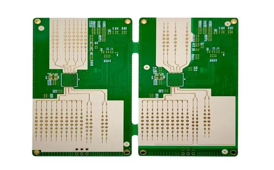
Thermal runaway in multilayer PCB design can lead to performance issues, component failure, or even complete system breakdowns. So, how do you prevent it? By mastering thermal management through strategic techniques like using thermal vias, optimizing heat sink placement, selecting materials with high thermal conductivity, running thermal simulations, and applying effective cooling methods. In this comprehensive guide, we’ll dive deep into each of these aspects to help you design multilayer PCBs that stay cool under pressure.
Whether you’re an electronics engineer or a PCB designer, managing heat in multilayer boards is crucial for reliability and efficiency. Let’s explore practical strategies and actionable tips to tackle thermal challenges and ensure your designs perform at their best.
Why Thermal Management Matters in Multilayer PCB Design
Multilayer PCBs are the backbone of modern electronics, packing complex circuitry into compact spaces. However, with more layers and components squeezed into smaller areas, heat generation becomes a significant concern. Excessive heat can degrade components, reduce lifespan, and cause signal integrity issues. Without proper thermal management, you risk thermal runaway—a condition where rising temperatures cause a feedback loop of increasing heat, potentially leading to catastrophic failure.
Effective thermal management ensures that heat is dissipated efficiently, maintaining optimal operating temperatures for components. This not only boosts performance but also extends the life of your PCB. Let’s break down the key techniques to achieve this, focusing on specific strategies tailored for multilayer designs.
Understanding Heat Sources in Multilayer PCBs
Before diving into solutions, it’s essential to identify where heat comes from in multilayer PCBs. Common sources include:
- Power Components: ICs, transistors, and voltage regulators often generate significant heat due to high current flow.
- High-Density Layouts: Crowded component placement limits airflow and traps heat.
- Inner Layers: Heat in internal layers struggles to escape due to limited exposure to external cooling.
- High-Frequency Signals: Rapid switching in high-speed circuits increases power dissipation and heat.
With these challenges in mind, let’s explore proven methods to manage heat effectively.
Thermal Vias in Multilayer PCBs: Your Heat Escape Route
One of the most effective ways to manage heat in multilayer PCBs is through the use of thermal vias. These are small, plated-through holes that act as conduits, transferring heat from hot spots on the surface or inner layers to a heat-dissipating layer or external cooling mechanism.
How Thermal Vias Work
Thermal vias are typically placed directly under or near high-heat components like power ICs. They connect to copper planes or pads that spread heat across a larger area or to the opposite side of the board, where it can be dissipated. For multilayer PCBs, thermal vias are especially critical because inner layers have no direct access to airflow or external cooling.
For example, a thermal via array under a component dissipating 5W of power can reduce its junction temperature by up to 20°C, depending on the via count, diameter, and copper thickness. A common practice is to use vias with a diameter of 0.3mm to 0.5mm, spaced in a grid pattern for maximum heat transfer.
Best Practices for Thermal Vias in Multilayer PCBs
- Placement: Position vias directly beneath heat-generating components for the shortest heat path.
- Density: Use multiple vias (e.g., a 4x4 grid) to increase thermal conductivity. More vias mean better heat dissipation.
- Connection: Connect vias to large copper planes on multiple layers to spread heat effectively.
- Filling: Consider filling vias with conductive epoxy to enhance thermal performance, though this increases manufacturing cost.
By integrating thermal vias strategically, you can significantly lower temperatures in critical areas of your multilayer PCB design.
Heat Sink Placement on PCBs: Maximizing Cooling Efficiency
Heat sinks are another powerful tool for thermal management, especially for components that generate substantial heat. Proper heat sink placement on PCBs can make a dramatic difference in temperature control, particularly in multilayer designs where space and airflow are limited.
Choosing the Right Heat Sink
Heat sinks come in various forms—passive (relying on natural convection) and active (using fans for forced airflow). For multilayer PCBs, compact heat sinks with high fin density are often ideal due to space constraints. Aluminum heat sinks, with a thermal conductivity of around 200 W/m·K, are a popular choice for their balance of cost and performance.
Optimal Heat Sink Placement on PCBs
- Direct Contact: Place the heat sink directly on top of the heat-generating component, using thermal interface materials (TIMs) like thermal paste or pads to reduce thermal resistance. A good TIM can lower thermal resistance to below 0.5°C/W.
- Orientation: Align heat sink fins with the direction of airflow in the system to maximize convection. For natural convection, vertical fins often perform better.
- Proximity to Edges: If possible, position heat sinks near board edges where airflow is less obstructed.
- Clearance: Ensure sufficient clearance around the heat sink to avoid blocking airflow to other components.
Proper heat sink placement can reduce component temperatures by 15-30°C, depending on the design and environment. Always consider the overall system airflow when deciding on placement.
PCB Material Thermal Conductivity: Building a Cool Foundation
The choice of materials in multilayer PCB design plays a critical role in thermal management. PCB material thermal conductivity determines how effectively heat can be conducted away from hot spots to cooler areas or external dissipators.
Common PCB Materials and Their Thermal Conductivity
Standard FR-4 material, widely used in PCB manufacturing, has a thermal conductivity of about 0.25 W/m·K, which is relatively low. For high-power applications, consider advanced materials:
- High-Tg FR-4: Offers slightly better thermal performance (around 0.3 W/m·K) and withstands higher temperatures.
- Metal-Core PCBs (MCPCBs): Use an aluminum or copper core with thermal conductivity up to 200 W/m·K, ideal for LED and power electronics.
- Ceramic-Based Materials: Provide thermal conductivity of 20-30 W/m·K and excellent heat resistance, though at a higher cost.
Layer Stackup and Copper Thickness
In multilayer PCBs, increasing copper thickness on power and ground planes enhances thermal conductivity. For instance, using 2 oz copper (70 μm thick) instead of 1 oz (35 μm) can improve heat spreading by nearly 50%. Additionally, dedicating inner layers as thermal planes connected to vias can create efficient heat dissipation paths.
Selecting materials with high thermal conductivity and optimizing your stackup design are foundational steps to prevent thermal issues in multilayer PCBs.
Thermal Simulation for PCBs: Predicting and Preventing Issues
Designing for thermal management isn’t just about applying techniques—it’s about predicting outcomes. Thermal simulation for PCBs allows you to model heat distribution, identify hot spots, and test solutions before manufacturing.
Benefits of Thermal Simulation
Thermal simulation tools use finite element analysis (FEA) to calculate temperature profiles across your PCB. By inputting parameters like component power dissipation (e.g., 3W for a specific IC), material properties, and ambient conditions (e.g., 25°C room temperature), you can visualize how heat flows through your design. This helps in:
- Locating hot spots that exceed safe operating temperatures (e.g., above 85°C for most ICs).
- Testing the effectiveness of thermal vias, heat sinks, and material choices.
- Reducing costly redesigns by catching issues early.
Steps to Perform Thermal Simulation for PCBs
- Define component power ratings and heat generation values.
- Input PCB stackup details, including layer materials and copper thickness.
- Set boundary conditions like ambient temperature and airflow speed (e.g., 1 m/s for forced convection).
- Analyze results to adjust via placement, heat sink size, or material selection.
Thermal simulation is a game-changer for multilayer PCB design, ensuring your thermal management strategies are effective before production.
Cooling Techniques for Multilayer PCBs: Beyond Vias and Heat Sinks
While thermal vias and heat sinks are essential, additional cooling techniques for multilayer PCBs can further enhance thermal performance. These methods address system-level cooling and complement board-level strategies.
Active Cooling with Fans
For high-power designs, active cooling using fans can significantly lower temperatures. Fans provide forced convection, moving air across heat sinks and components at speeds like 2-5 m/s, reducing temperatures by 20-40°C compared to natural convection. Place fans to direct airflow over critical areas, and ensure vents in enclosures don’t obstruct air paths.
Heat Pipes and Vapor Chambers
Heat pipes transfer heat efficiently over long distances using phase-change cooling. With effective thermal conductivity up to 10,000 W/m·K, they’re ideal for moving heat from inner layers or crowded areas to external dissipators. Vapor chambers, a flat version of heat pipes, spread heat uniformly across a plane, useful for large components.
Enclosure Design for Airflow
The enclosure housing your PCB impacts cooling. Design enclosures with vents or perforations near heat sources to promote natural convection. For compact systems, consider cutouts aligned with heat sinks to improve airflow.
Combining these cooling techniques with board-level solutions ensures comprehensive thermal management for multilayer PCBs, even in demanding applications.
Practical Tips for Implementing Thermal Management
To wrap up, here are actionable tips to integrate thermal management into your multilayer PCB design process:
- Start with thermal analysis during the schematic phase to identify high-power components early.
- Use a combination of thermal vias, heat sinks, and material choices tailored to your design’s heat load.
- Run thermal simulations to validate your design under worst-case conditions (e.g., maximum power and ambient temperature of 40°C).
- Collaborate with your manufacturing partner to balance thermal performance with cost, especially for advanced materials or via filling.
- Monitor real-world performance post-production using temperature sensors to ensure simulations match reality.
Conclusion: Stay Cool with Effective Thermal Management
Thermal runaway doesn’t have to be a threat to your multilayer PCB designs. By mastering thermal management techniques like using thermal vias in multilayer PCBs, optimizing heat sink placement on PCBs, selecting materials with high PCB material thermal conductivity, leveraging thermal simulation for PCBs, and applying cooling techniques for multilayer PCBs, you can keep temperatures in check and ensure reliable performance.
At ALLPCB, we’re committed to supporting your design journey with resources and expertise to tackle thermal challenges. Implement these strategies in your next project to build robust, efficient multilayer PCBs that stand up to the heat.
 ALLPCB


