ALLPCB


If you're looking to design a network switch PCB layout that ensures high performance and reliability, you've come to the right place. This guide covers everything from essential design guidelines to the manufacturing process, including SMT assembly and through-hole technology. Whether you're an engineer or a project manager, we'll walk you through the critical steps to create a robust network switch PCB that meets modern networking demands.
In the sections below, we'll dive deep into the intricacies of PCB design for network switches, offering practical tips, technical insights, and step-by-step processes to take your project from concept to production. Let’s get started!
What is a Network Switch PCB Layout and Why Does It Matter?
A network switch PCB (Printed Circuit Board) layout is the foundation of a network switch—a device that connects multiple devices in a network, directing data traffic efficiently. The PCB layout determines how components like Ethernet controllers, power regulators, and connectors are arranged and connected, directly impacting the switch’s performance, signal integrity, and durability.
A well-designed network switch PCB layout ensures minimal signal interference, efficient power distribution, and reliable high-speed data transfer, often exceeding 1 Gbps in modern switches. Poor design, on the other hand, can lead to issues like crosstalk, electromagnetic interference (EMI), or overheating, which can disrupt network performance. With the right approach, you can avoid these pitfalls and build a product that stands out in today’s fast-paced tech landscape.
Key Principles of Network Switch PCB Design Guidelines
Designing a PCB for a network switch requires careful planning and adherence to specific guidelines. Here are the core principles to follow for optimal results:
1. Understand the Requirements
Before starting the design, define the specifications of your network switch. Consider factors like the number of ports (e.g., 8, 16, or 24 ports), data speed (1 Gbps or 10 Gbps), and power requirements (e.g., PoE—Power over Ethernet—support). These specs will guide your component selection and layout decisions.
For instance, a 24-port switch supporting 10 Gbps speeds requires high-speed signal routing and robust power management to handle the load. Knowing these details upfront helps in choosing the right materials and layer stack-up for your PCB.

2. Layer Stack-Up for Signal Integrity
Network switches often handle high-speed signals, so a proper layer stack-up is critical. A typical design might use a 4-layer or 6-layer PCB, with dedicated layers for power, ground, and signal routing. For example:
- Top Layer: Components and high-speed signal traces.
- Ground Plane: Reduces EMI and provides a stable reference for signals.
- Power Plane: Distributes power evenly to components.
- Bottom Layer: Additional routing or ground.
Ensure controlled impedance for high-speed traces, often targeting 50 ohms for single-ended signals or 100 ohms for differential pairs, to prevent signal degradation.
3. Component Placement for Efficiency
Place components logically to minimize trace lengths and avoid interference. Group related components, such as Ethernet PHYs near RJ45 connectors, to reduce signal delays. Keep power components like voltage regulators away from sensitive signal areas to avoid noise coupling.
Also, consider thermal management. High-power components should be placed near heat sinks or ventilation areas to prevent overheating, especially in PoE-enabled switches that can dissipate over 30W per port.
4. Routing High-Speed Signals
High-speed signals in network switches, such as those between the switch IC and Ethernet ports, require careful routing. Follow these tips:
- Avoid sharp bends in traces; use 45-degree angles to reduce signal reflection.
- Maintain equal trace lengths for differential pairs to prevent timing skew, ideally within 5 mils (0.005 inches) of each other.
- Keep traces away from noisy areas like power lines to minimize crosstalk.

5. Power Distribution and Decoupling
A stable power supply is vital for network switches. Use wide traces or power planes to handle current loads, especially for PoE designs that may require up to 2A per port. Place decoupling capacitors (e.g., 0.1 μF ceramic capacitors) close to IC power pins to filter noise and stabilize voltage levels, typically within 100 mils of the pin.
The PCB Manufacturing Process for Network Switches
Once your network switch PCB layout is finalized, the next step is manufacturing. This process transforms your design into a physical board ready for assembly. Here’s a breakdown of the key stages:
1. Design File Preparation
Export your design files, including Gerber files, drill files, and a Bill of Materials (BOM). These files contain all the information needed for fabrication, such as layer details, trace patterns, and component placements. Double-check for errors like missing vias or incorrect pad sizes to avoid costly delays.
2. PCB Fabrication
Fabrication involves creating the bare PCB based on your design. The process includes:
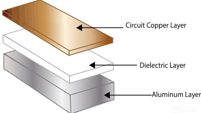
- Material Selection: Common materials like FR-4 are used for standard designs, while high-speed switches may require low-loss materials like Rogers for better signal integrity.
- Layer Lamination: Multiple layers are stacked and bonded together under heat and pressure.
- Etching: Copper is removed from non-conductive areas to form traces and pads.
- Drilling: Holes are drilled for vias and through-hole components.
- Surface Finish: A protective coating like HASL or ENIG is applied to prevent oxidation and ensure solderability.

3. Quality Checks
After fabrication, the PCB undergoes testing for defects. Electrical tests check for shorts or open circuits, while visual inspections ensure alignment and surface quality. For high-speed network switches, impedance testing may be conducted to verify that traces meet the specified values, such as 50 ohms.
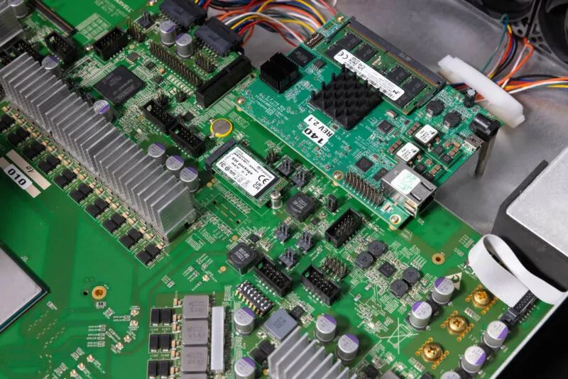
SMT Assembly for Network Switch PCBs
Surface Mount Technology (SMT) assembly is the preferred method for modern network switch PCBs due to its efficiency and ability to handle small, high-density components. Here’s how it works:
1. Solder Paste Application
Solder paste, a mixture of tiny solder particles and flux, is applied to the PCB pads using a stencil. This ensures precise placement for surface-mount components like resistors, capacitors, and ICs.
2. Component Placement
Automated pick-and-place machines position components onto the solder paste with high accuracy, often placing thousands of components per hour. For a network switch, this includes tiny chips like 0402 resistors or complex BGA (Ball Grid Array) packages for the main switch IC.
3. Reflow Soldering
The PCB passes through a reflow oven, where heat melts the solder paste, forming strong electrical connections between components and pads. The temperature profile typically peaks at around 245°C for lead-free solder, ensuring reliable joints without damaging components.
4. Inspection and Testing
After assembly, Automated Optical Inspection (AOI) systems check for misaligned components or soldering defects. For critical network switch PCBs, X-ray inspection may be used to verify connections under BGA packages. Functional testing ensures the board operates as intended, often involving data throughput tests at speeds like 1 Gbps or higher.
Through-Hole Technology in Network Switch PCBs
While SMT dominates modern designs, Through-Hole Technology (THT) is still used in network switch PCBs for components requiring high mechanical strength, such as connectors and power inductors. Here’s an overview of the process:
1. Component Insertion
Through-hole components, with their long leads, are inserted into pre-drilled holes on the PCB. This can be done manually for prototypes or with automated machines for larger runs.
2. Soldering
Wave soldering is commonly used for through-hole components. The PCB passes over a wave of molten solder, typically at 260°C, which bonds the leads to the pads. For smaller batches, hand soldering may be used for precision.
3. Benefits and Limitations
Through-hole components offer strong mechanical bonds, ideal for RJ45 connectors in network switches that endure frequent plugging and unplugging. However, they take up more space and are slower to assemble compared to SMT, making them less common in high-density designs.

Challenges in Network Switch PCB Layout and How to Overcome Them
Designing and manufacturing a network switch PCB comes with unique challenges. Here are a few common issues and solutions:
1. Signal Integrity at High Speeds
High-speed data rates (e.g., 10 Gbps) can lead to signal loss or crosstalk. Use controlled impedance routing, proper termination resistors (e.g., 50 ohms), and keep trace lengths short to mitigate these issues.
2. Thermal Management
Network switches with PoE can generate significant heat, with power dissipation exceeding 100W in some designs. Incorporate thermal vias, heat sinks, and adequate spacing around high-power components to manage heat effectively.
3. EMI and Noise
Electromagnetic interference can disrupt network performance. Use ground planes, shield sensitive areas, and follow proper decoupling practices to minimize noise.
Final Steps: Testing and Deployment
Before mass production, prototype testing is crucial. Conduct stress tests to simulate real-world conditions, such as continuous data transfer at maximum capacity (e.g., 24 ports at 1 Gbps). Measure key metrics like packet loss, latency, and power consumption to ensure the design meets expectations.
Once testing is complete, move to full-scale production with a trusted manufacturing partner. Ensure clear communication regarding design files, assembly requirements, and quality standards to avoid errors during scaling.
Conclusion: Building a Reliable Network Switch PCB
Creating a network switch PCB layout that performs reliably requires attention to detail at every stage—from design guidelines to manufacturing processes like SMT assembly and through-hole technology. By following best practices for signal integrity, power distribution, and thermal management, you can build a product that meets the demands of modern networking environments.
Whether you're designing for a small office switch or an industrial-grade solution, the principles covered in this guide provide a solid foundation. With careful planning and execution, your network switch PCB will deliver seamless connectivity and long-term reliability. Start applying these insights to your next project and see the difference a well-designed PCB can make!