ALLPCB


When designing a printed circuit board (PCB), one of the critical decisions you'll face is choosing the right power plane fill type. Should you go with a solid power plane or a hatched power plane? Both options have their unique advantages and drawbacks, and the choice can significantly impact your PCB's performance, manufacturing process, and cost. In this detailed guide, we'll break down the differences between solid and hatched power plane fills, explore copper pour advantages, and help you decide which is best for your specific project.
At a high level, a solid power plane offers better current-carrying capacity, improved thermal dissipation, and enhanced electromagnetic interference (EMI) shielding, making it ideal for high-power or high-speed designs. On the other hand, a hatched power plane reduces the amount of copper used, which can lower manufacturing costs and minimize warping during production, often suiting simpler or cost-sensitive projects. Let's dive deeper into these power plane fill types to understand their applications in PCB manufacturing.
What Are Power Plane Fills and Why Do They Matter?
Power plane fills, often referred to as copper pours, are areas on a PCB layer filled with copper to distribute power or ground signals across the board. These fills create a low-impedance path for current, reduce noise, and improve signal integrity. They are especially crucial in multilayer PCBs where dedicated layers are used for power and ground distribution.
The type of fill—solid or hatched—directly affects how the PCB handles electrical performance, heat, and manufacturing challenges. A poorly chosen power plane fill can lead to issues like voltage drops, overheating, or increased EMI, which can compromise the reliability of your design. Understanding the nuances of each type is key to optimizing your PCB for performance and cost.
Solid Power Plane: Features and Benefits
A solid power plane is a continuous, unbroken layer of copper that covers an entire area or layer of the PCB, typically used for power or ground distribution. This type of fill is common in modern PCB designs due to its robust electrical and thermal properties.
Key Advantages of Solid Power Planes
- Low Impedance and High Current Capacity: A solid copper layer provides a wide, uninterrupted path for current flow, reducing resistance and voltage drops. For example, a solid power plane can handle currents in the range of several amperes without significant losses, making it ideal for high-power applications.
- Improved EMI Shielding: The continuous copper acts as a shield, minimizing electromagnetic interference. This is critical for high-speed digital circuits where signal integrity is paramount. Studies show that solid planes can reduce EMI by up to 20-30% compared to hatched fills in certain frequency ranges.
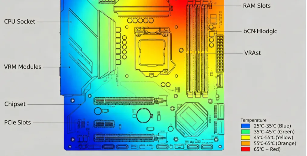
- Better Thermal Dissipation: Solid copper distributes heat more evenly across the board, preventing hotspots. This is especially useful in designs with power-intensive components, as it can reduce peak temperatures by 10-15°C in some cases.
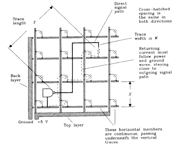
- Enhanced Signal Integrity: For high-speed signals (e.g., above 100 MHz), a solid ground plane reduces return path inductance, ensuring cleaner signal transmission and less crosstalk.
Potential Drawbacks
- Higher Copper Usage: Solid fills require more copper, which can increase material costs, especially for large boards.
- Risk of Warping: During manufacturing, large areas of solid copper can cause uneven thermal expansion, leading to board warping if not balanced with copper on other layers.
- Etching Challenges: Removing excess copper during the etching process can be more time-consuming and may require more etching fluid, potentially impacting production costs.
Suggested Image Placement: Insert an image here showing a thermal simulation of a solid power plane dissipating heat across a PCB. ALT Text: "Thermal simulation of heat dissipation on a solid power plane in PCB design."
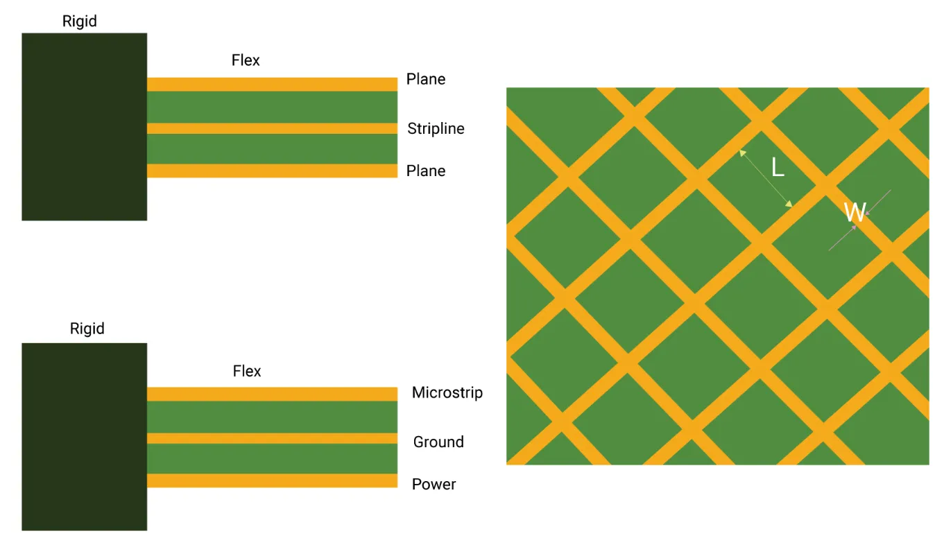
Hatched Power Plane: Features and Benefits
A hatched power plane, sometimes called a crosshatched or grid fill, consists of a pattern of copper lines or grids rather than a continuous layer. This design was more common in older PCBs but still has relevance in specific applications today.
Key Advantages of Hatched Power Planes
- Reduced Copper Usage: By using less copper, hatched fills lower material costs and reduce the amount of etching fluid needed during manufacturing. This can save up to 30-50% of copper compared to solid fills on large boards.
- Minimized Warping: The grid pattern allows for more even thermal expansion during soldering and reflow processes, reducing the risk of board deformation. This is particularly beneficial for thin or flexible PCBs.
- Cost-Effective for Simpler Designs: In low-power or low-speed applications (e.g., below 50 MHz), a hatched plane can provide adequate performance without the added expense of a solid fill.
- Easier Manufacturing: Less copper means faster etching times and less strain on manufacturing equipment, which can speed up production for simpler boards.
Potential Drawbacks
- Higher Impedance: The discontinuous copper pattern increases resistance and inductance, leading to potential voltage drops. For instance, a hatched plane might exhibit impedance values 2-3 times higher than a solid plane under similar conditions.
- Poor EMI Shielding: The gaps in the copper grid allow more electromagnetic interference to pass through, which can degrade signal quality in high-speed or RF designs.
- Limited Thermal Performance: With less copper to spread heat, hatched planes are less effective at thermal management, potentially leading to localized overheating in power-intensive designs.
Copper Pour Advantages in PCB Design
Regardless of whether you choose a solid or hatched power plane, implementing a copper pour in your PCB design offers several inherent benefits. Copper pour refers to filling unused areas of a PCB with copper, typically connected to power or ground nets. Let's explore why copper pours are a staple in modern PCB manufacturing.
- Enhanced Electrical Performance: Copper pours reduce loop inductance and provide a stable reference plane for signals, improving overall circuit performance. This is especially critical for designs operating at high frequencies (e.g., 500 MHz and above).
- Noise Reduction: A well-designed copper pour minimizes ground bounce and crosstalk, ensuring cleaner power delivery to components.
- Manufacturing Efficiency: Filling unused areas with copper reduces the amount of etching required, as less copper needs to be removed. This can lower production costs by up to 10-15% in some cases.
- Mechanical Stability: Copper pours help balance the copper distribution across layers, reducing the likelihood of warping or delamination during manufacturing.
By leveraging these copper pour advantages, designers can create more reliable and cost-effective PCBs tailored to their project needs.
Solid vs. Hatched: Comparing Key Factors
Choosing between a solid and hatched power plane depends on several factors, including electrical requirements, thermal management, cost constraints, and manufacturing considerations. Below is a detailed comparison to help you make an informed decision.
| Criteria | Solid Power Plane | Hatched Power Plane |
|---|---|---|
| Current Capacity | High (e.g., supports 5-10A with minimal voltage drop) | Moderate (e.g., limited to 1-3A before significant losses) |
| EMI Shielding | Excellent (reduces EMI by 20-30%) | Poor (gaps allow interference) |
| Thermal Dissipation | Superior (reduces peak temperatures by 10-15°C) | Limited (higher risk of hotspots) |
| Cost | Higher (more copper and etching fluid) | Lower (up to 30-50% less copper) |
| Manufacturing Risk | Higher risk of warping if unbalanced | Lower risk due to even thermal expansion |
When to Use Solid Power Planes
Solid power planes are the go-to choice for most modern PCB designs, especially in the following scenarios:
- High-Power Applications: If your design involves high current loads (e.g., power supplies or motor drivers), a solid plane ensures minimal voltage drops and stable power delivery.
- High-Speed Digital Circuits: For applications with fast-switching signals (e.g., microprocessors or DDR memory), solid planes provide a low-inductance return path, reducing noise and crosstalk.
- RF and Wireless Designs: Solid ground planes are critical for minimizing EMI and maintaining signal integrity in radio frequency circuits.
- Thermal Management Needs: If your board includes heat-generating components, a solid plane helps spread heat evenly, protecting sensitive parts.
When to Use Hatched Power Planes
Hatched power planes are less common today but still have their place in specific situations:
- Cost-Sensitive Projects: For low-budget designs where performance requirements are minimal, a hatched fill can save on material and manufacturing costs.
- Low-Power or Analog Designs: If your circuit operates at low frequencies (e.g., under 50 MHz) and doesn't require extensive EMI shielding, a hatched plane may suffice.
- Flexible PCBs: Hatched fills are often used in flex PCBs to reduce stress and prevent cracking during bending, as solid copper can be too rigid.
- Prototyping or Testing: During early design stages, a hatched plane can be a cost-effective way to test basic functionality before committing to a solid fill.
Best Practices for Power Plane Design in PCB Manufacturing
Whether you choose a solid or hatched power plane, following best practices in PCB manufacturing can optimize your design for performance and reliability. Here are some actionable tips:
- Balance Copper Distribution: Ensure that copper is evenly distributed across layers to prevent warping. For solid planes, match copper coverage on opposing layers to maintain thermal balance.
- Use Thermal Reliefs: When connecting pads to a power plane, use thermal reliefs (spokes of copper) to prevent soldering issues caused by excessive heat sinking into the plane.
- Maintain Clearances: Keep a sufficient standoff distance (e.g., 8-10 mils) between the power plane and unrelated tracks or pads to avoid short circuits.
- Simulate Performance: Use PCB design software to simulate current flow, thermal distribution, and EMI before finalizing your power plane fill type. This can help identify potential issues early.
- Consult with Manufacturers: Work closely with your PCB fabrication team to understand their capabilities and constraints, especially for solid fills that may require specific etching processes.
Conclusion: Making the Right Choice for Your PCB
Deciding between a solid power plane and a hatched power plane ultimately comes down to the specific needs of your PCB design. If performance, signal integrity, and thermal management are priorities—such as in high-speed or high-power applications—a solid power plane is likely the better choice. However, for cost-sensitive or simpler designs where electrical demands are lower, a hatched power plane can be a practical and economical option.
By understanding the trade-offs and copper pour advantages, you can tailor your power plane fill to match your project's requirements. Remember to consider factors like current capacity, EMI shielding, thermal performance, and manufacturing constraints when making your decision. With the right approach, you'll create a PCB that balances performance, reliability, and cost effectively.