 ALLPCB


In the world of PCB design, electromagnetic interference (EMI) can be a major hurdle, especially when it comes to power planes. If you're looking to reduce power plane EMI and shield your PCB effectively, you've come to the right place. This blog will dive into practical solutions for power plane EMI, electromagnetic interference shielding, and PCB shielding techniques. We'll also cover how to minimize radiated emissions and the importance of proper power plane grounding. Let's explore actionable strategies to ensure your designs are robust and interference-free.
Understanding Power Plane EMI and Its Impact on PCB Design
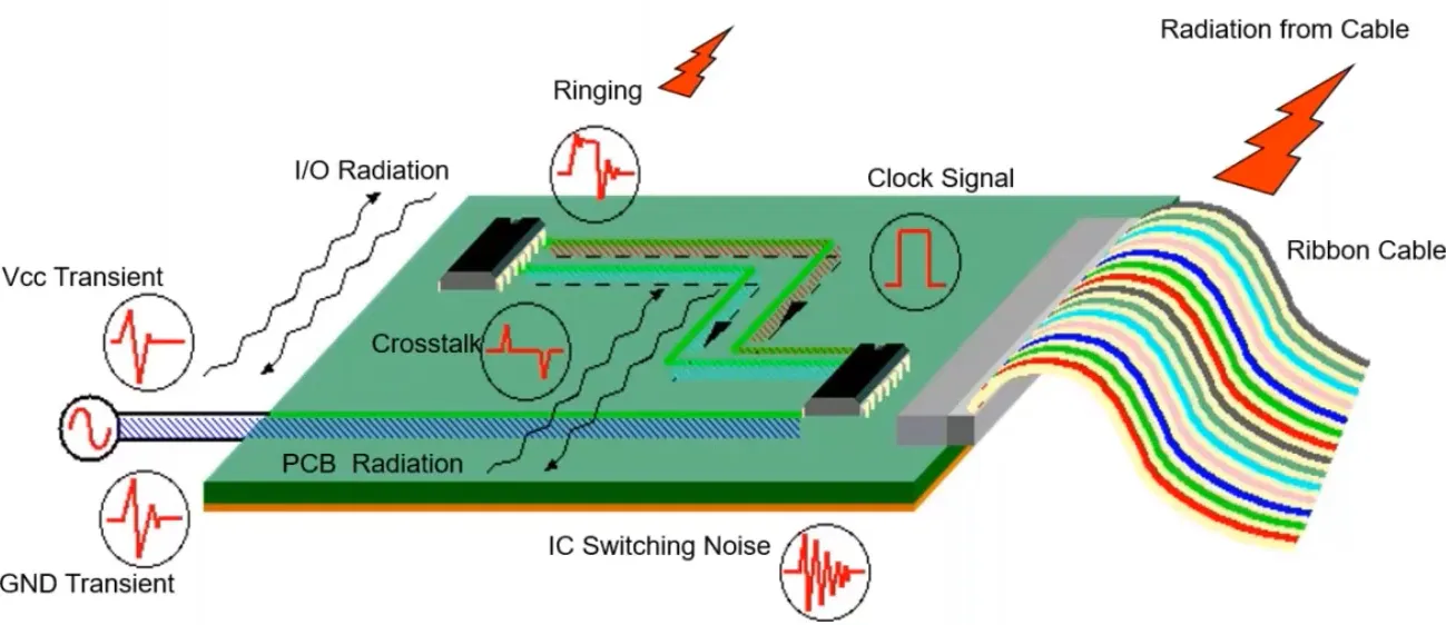
Electromagnetic interference, or EMI, occurs when unwanted electrical noise disrupts the performance of electronic circuits. In PCB design, the power plane—a large conductive layer that distributes power to components—can act as both a source and a victim of EMI. High-speed signals, switching regulators, and nearby components can induce noise in the power plane, leading to issues like signal distortion, data errors, or even complete system failure.
Power plane EMI often manifests as radiated emissions, where electromagnetic waves escape the board and interfere with other devices, or as conducted emissions, where noise travels through power lines. With modern electronics becoming faster and more compact, managing power plane EMI is critical to meeting regulatory standards and ensuring reliable operation.
In this guide, we'll break down proven methods to tackle EMI, focusing on shielding techniques and grounding practices. Whether you're designing for consumer electronics, industrial systems, or automotive applications, these tips will help you build cleaner, more efficient PCBs.
Why Power Plane EMI Matters in Modern Electronics
As electronic devices shrink in size and operate at higher frequencies (often exceeding 1 GHz), the risk of EMI increases. A poorly designed power plane can act like an antenna, broadcasting noise that affects nearby circuits or external devices. This is especially problematic in densely packed boards where components are placed closer together, amplifying the potential for interference.
For instance, a power plane with inadequate grounding might resonate at certain frequencies, creating voltage fluctuations as high as 100 mV or more. These fluctuations can degrade signal integrity, especially for sensitive analog circuits or high-speed digital signals operating at 2.5 Gbps or faster. By addressing power plane EMI, you not only improve your board's performance but also ensure compliance with strict EMC (electromagnetic compatibility) regulations.
Key Techniques for Power Plane EMI Reduction
Reducing EMI starts with thoughtful design practices. Below, we outline several proven strategies to minimize noise in your power plane and shield your PCB from interference.
1. Optimize Power Plane Grounding
Proper power plane grounding is the foundation of EMI reduction. A well-designed ground plane acts as a low-impedance return path for currents, reducing noise and preventing the power plane from radiating emissions. Here are some tips to achieve this:
- Create a Solid Ground Plane: Use a continuous ground plane directly beneath the power plane to form a low-inductance path. Avoid splitting the ground plane unless absolutely necessary, as splits can increase loop inductance and EMI.
- Use Multiple Vias: Connect the ground plane to component ground pins with multiple vias. This reduces impedance and minimizes ground bounce, which can contribute to radiated emissions. Aim for via spacing of less than 1/20th of the wavelength of your highest frequency signal (e.g., for a 1 GHz signal, space vias less than 7.5 mm apart).
- Stitch Ground Planes: For multilayer boards, stitch ground planes together with vias around the board's edges. This creates a Faraday cage-like effect, containing EMI within the board.
By focusing on power plane grounding, you can significantly cut down on noise. For example, studies show that a well-stitched ground plane can reduce radiated emissions by up to 20 dB at frequencies above 100 MHz.
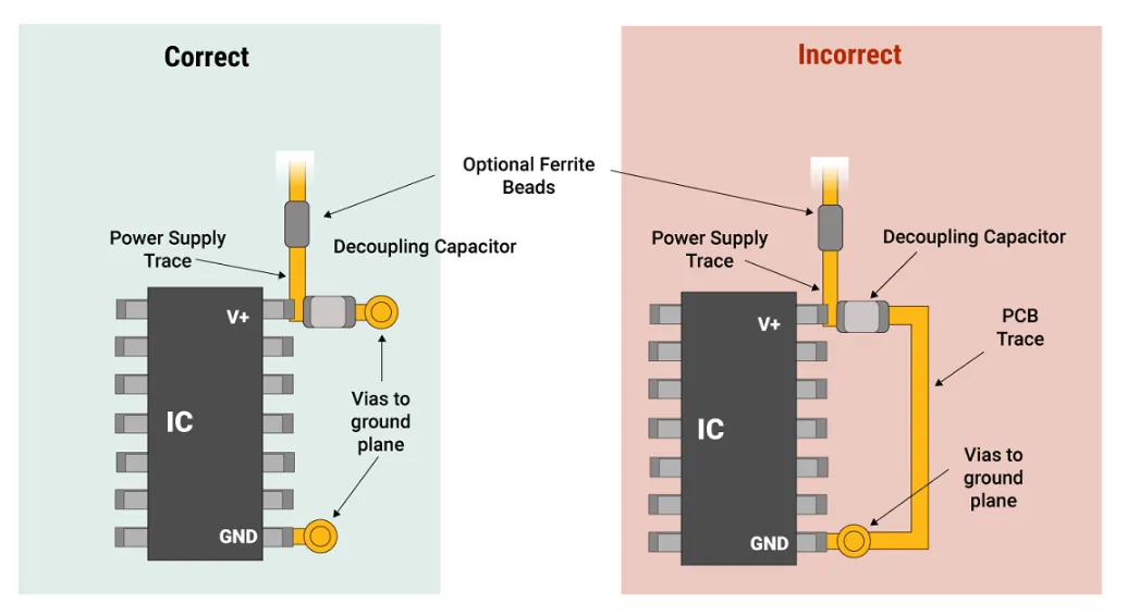
2. Implement Decoupling Capacitors Effectively
Decoupling capacitors are essential for stabilizing the power plane and filtering out high-frequency noise. When placed correctly, they act as local energy reservoirs, reducing voltage ripples caused by switching components like microcontrollers or FPGAs.
- Choose the Right Capacitor Values: Use a mix of capacitor values (e.g., 0.1 μF, 1 μF, and 10 μF) to cover a wide frequency range. Smaller capacitors handle higher frequencies (up to 100 MHz), while larger ones address lower-frequency noise.
- Place Capacitors Close to ICs: Position decoupling capacitors as close as possible to the power pins of integrated circuits. A placement distance of less than 2 mm can reduce parasitic inductance, improving noise suppression.
- Minimize Loop Area: Route power and ground traces to capacitors with minimal loop area to avoid creating unintended antennas that radiate EMI.
3. Use Split Power Planes Strategically
While a continuous power plane is ideal for uniform power distribution, splitting the power plane can help isolate noisy components from sensitive ones. For example, separate the power plane for a high-speed digital circuit from an analog circuit to prevent noise coupling.
- Bridge Splits with Inductors or Ferrite Beads: Use inductors or ferrite beads to connect split planes, allowing DC power to flow while blocking high-frequency noise. A ferrite bead with a current rating of 1 A and impedance of 600 ohms at 100 MHz is often effective.
- Avoid Signal Crossing Splits: Ensure signal traces do not cross power plane splits, as this can create EMI and disrupt return paths.
Splitting planes requires careful planning, but when done right, it can reduce noise coupling by as much as 15 dB in mixed-signal designs.
Electromagnetic Interference Shielding for PCBs
Beyond power plane design, electromagnetic interference shielding plays a vital role in protecting your PCB from external and internal noise. Shielding techniques focus on containing or blocking electromagnetic fields to prevent interference.
1. Enclose Sensitive Areas with Shielding Cans
Shielding cans, or metal enclosures, are often used to cover sensitive components like RF circuits or high-speed oscillators. These cans block external EMI and prevent internal emissions from escaping.
- Material Choice: Use materials like aluminum or steel with high conductivity for effective shielding. A thickness of 0.5 mm is usually sufficient for frequencies below 1 GHz.
- Grounding the Can: Connect the shielding can to the ground plane with multiple points to ensure low impedance and prevent gaps that could leak EMI.
Shielding cans can reduce radiated emissions by up to 30 dB, making them a powerful tool for PCB shielding techniques.
2. Use Guard Rings for Sensitive Traces
Guard rings are grounded traces that surround sensitive signal lines, acting as a barrier against EMI. They are particularly useful for protecting analog signals or clock lines from power plane noise.
- Placement: Place guard rings on the same layer as the protected trace, encircling it completely if possible.
- Ground Connection: Connect the guard ring to ground at multiple points to maintain low impedance.
This technique can lower noise pickup by 10-15 dB, especially in high-frequency designs.
Reducing Radiated Emissions in PCB Design
Reducing radiated emissions is a critical goal in EMI management. Radiated emissions occur when electromagnetic energy escapes the board, often due to poor layout or inadequate shielding. Here are some practical ways to tackle this issue:
1. Minimize Loop Areas in Layout
Large current loops in your PCB layout can act as antennas, radiating EMI. To reduce this:
- Shorten Trace Lengths: Keep power and signal traces as short as possible to minimize loop areas. For high-speed signals above 100 MHz, aim for trace lengths under 10 mm where feasible.
- Route Traces Over Ground Planes: Ensure signal traces are routed over a solid ground plane to provide a low-impedance return path and reduce radiation.
2. Control Edge Effects
The edges of a PCB can radiate EMI if not managed properly. To mitigate this:
- Add Ground Stitching Vias: Place vias along the PCB edges to connect ground planes, reducing edge radiation by up to 10 dB.
- Avoid Components Near Edges: Keep high-speed components and traces away from board edges to prevent unintended radiation.
Advanced Tips for Power Plane EMI Reduction
For complex designs, consider these advanced strategies to further reduce power plane EMI:
- Use Embedded Capacitance: Some multilayer PCBs incorporate thin dielectric layers between power and ground planes to create embedded capacitance. This can reduce noise at frequencies up to 500 MHz, acting as a distributed decoupling capacitor.
- Simulate EMI Early: Use simulation tools to model power plane impedance and identify resonance frequencies. Addressing issues in simulation can save costly redesigns later.
- Filter Power Entry Points: Place EMI filters or transient voltage suppressors at power entry points to block external noise from entering the board. A filter with a cutoff frequency of 10 MHz can be effective for most applications.
Conclusion: Building EMI-Resistant PCBs with Power Plane Optimization
Reducing power plane EMI and implementing effective electromagnetic interference shielding are essential for creating reliable, high-performance PCBs. By focusing on solid power plane grounding, strategic decoupling, and robust PCB shielding techniques, you can minimize noise and control radiated emissions. These practices not only improve your design's performance but also ensure compliance with EMC standards, saving time and cost in the long run.
Start by reviewing your current designs for potential EMI issues. Apply the tips shared in this blog, from optimizing grounding to using shielding cans, and watch as your boards become more resilient to interference. With careful planning and attention to detail, you can master the art of EMI reduction and build PCBs that stand up to the challenges of modern electronics.


