 ALLPCB


In the fast-paced world of networking, designing a high-performance network switch requires careful attention to the printed circuit board (PCB) layout. One of the most critical aspects is the PCB stack-up, which directly impacts signal integrity, especially in high-speed designs. If you're searching for ways to optimize your network switch PCB layer stack for better performance, you're in the right place. This blog uncovers the secrets of crafting a PCB stack-up that ensures excellent signal integrity in network switches, with a focus on high-speed PCB design, PCB stackup impedance control, and controlled impedance PCB techniques.
Let’s dive into the details of how a well-designed stack-up can make or break your network switch performance, and provide you with actionable tips to achieve optimal results.
What is a PCB Stack-Up and Why Does It Matter for Network Switches?
A PCB stack-up refers to the arrangement of conductive copper layers and insulating dielectric materials in a multilayer PCB. In a network switch, where data signals often travel at gigabit speeds (up to 10 Gbps or more), the stack-up design determines how well these signals maintain their quality without interference or loss. Poor stack-up design can lead to issues like crosstalk, electromagnetic interference (EMI), and signal degradation, all of which compromise the switch’s reliability.
For high-speed PCB design, the stack-up is the foundation of signal integrity in network switches. It affects impedance, signal routing, and power distribution. A well-planned network switch PCB layer stack ensures that high-speed signals travel with minimal distortion, while also managing heat and power delivery effectively.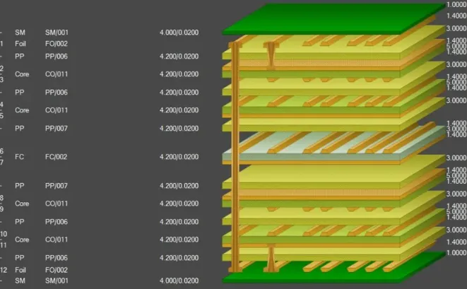
Key Challenges in Network Switch PCB Design
Before we explore the secrets of an optimized stack-up, let’s understand the challenges in designing a PCB for network switches:
- High-Speed Signals: Network switches handle data rates from 1 Gbps to 100 Gbps, requiring precise control over signal paths to avoid delays or reflections.
- Crosstalk: Adjacent signal traces can interfere with each other, especially at high frequencies, leading to data errors.
- Impedance Mismatches: Incorrect impedance in signal traces can cause signal reflections, degrading performance.
- EMI: High-speed signals can emit electromagnetic interference, affecting nearby components or violating regulatory standards.
Addressing these challenges starts with a carefully designed network switch PCB layer stack that prioritizes signal integrity in network switches.
Secrets to Designing an Optimal Network Switch PCB Stack-Up
Now, let’s uncover the key strategies for creating a PCB stack-up that supports high-speed performance and signal integrity.
1. Choose the Right Number of Layers
The number of layers in a PCB stack-up depends on the complexity of the network switch. For simpler designs handling speeds up to 1 Gbps, a 4-layer or 6-layer PCB may suffice. However, for switches supporting 10 Gbps or higher, an 8-layer, 10-layer, or even 12-layer stack-up is often necessary to separate high-speed signals, power planes, and ground planes effectively.
For example, a typical 8-layer stack-up for a network switch might look like this:
- Layer 1: Top Signal (High-Speed Traces)
- Layer 2: Ground Plane
- Layer 3: Signal Layer
- Layer 4: Power Plane
- Layer 5: Power Plane
- Layer 6: Signal Layer
- Layer 7: Ground Plane
- Layer 8: Bottom Signal
This arrangement ensures that high-speed signals on the top and bottom layers are close to ground planes, reducing EMI and improving signal return paths.
2. Prioritize Ground Planes for Signal Integrity
Ground planes are critical for maintaining signal integrity in network switches. They provide a low-impedance return path for high-speed signals, minimizing loop inductance and reducing EMI. Place a continuous ground plane directly below or above high-speed signal layers to ensure a stable reference.
For instance, in high-speed designs with signals running at 10 Gbps, the ground plane helps keep the signal’s return current close to the trace, reducing the loop area and preventing crosstalk. Avoid splitting ground planes under high-speed traces, as this can disrupt the return path and cause signal reflections.
3. Implement Controlled Impedance for High-Speed Traces
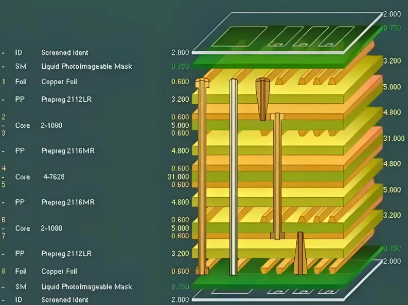
PCB stackup impedance control is a cornerstone of high-speed PCB design. Impedance mismatches in signal traces can cause reflections, leading to data errors in network switches. To achieve a controlled impedance PCB, you must carefully design trace widths, spacing, and dielectric thickness based on the target impedance, often 50 ohms for single-ended signals or 100 ohms for differential pairs in high-speed designs.
For example, a typical differential pair for a 10 Gbps Ethernet signal might require a trace width of 5 mils and a spacing of 8 mils on a specific dielectric material with a constant (Dk) of 3.8. Use impedance calculators or simulation tools during the design phase to verify these values based on your stack-up.
Additionally, ensure that the dielectric material between layers is uniform to avoid variations in impedance. Work closely with your PCB manufacturer to select materials with consistent dielectric properties for controlled impedance PCB designs.
4. Separate Power and Signal Layers Strategically
Power planes distribute voltage to components, but they can also introduce noise if not isolated from signal layers. In a network switch PCB layer stack, place power planes in the middle of the stack-up, sandwiched between ground planes, to minimize interference with high-speed signals on the outer layers.
For example, in a 10-layer stack-up, you might allocate layers 4 and 5 for power distribution, with ground planes on layers 3 and 6 to shield signals on layers 1, 2, 7, and 8. This setup reduces noise coupling and enhances signal integrity in network switches.
5. Minimize Via Usage in High-Speed Paths
Vias, which connect traces between layers, can introduce impedance discontinuities and signal reflections in high-speed designs. In high-speed PCB design, limit the number of vias in critical signal paths. If vias are unavoidable, use back-drilling techniques to remove unused via stubs, which can act as antennas and degrade signal quality at frequencies above 5 GHz.
For network switches handling 25 Gbps signals, even a small via stub can cause significant signal loss. Plan your routing to keep high-speed traces on a single layer whenever possible, or use blind and buried vias for cleaner transitions.
6. Optimize Layer Thickness and Material Selection
The thickness of dielectric layers and the choice of materials play a big role in PCB stackup impedance control. Thinner dielectric layers between signal and ground planes reduce loop inductance, improving signal integrity. However, they also increase capacitance, which may not be ideal for all designs.
For high-speed network switches, consider using low-loss dielectric materials like Rogers or Isola, which maintain stable dielectric constants at high frequencies (above 10 GHz). Standard FR-4 materials may suffice for lower-speed designs (up to 1 Gbps), but they often exhibit higher signal loss at gigabit speeds.
For instance, a dielectric thickness of 5 mils between a signal layer and ground plane can help achieve a 50-ohm impedance for a 6-mil-wide trace. Collaborate with your PCB fabricator to balance cost and performance when selecting materials and thicknesses.
Best Practices for Signal Integrity in Network Switches
Beyond stack-up design, several practices can further enhance signal integrity in network switches:
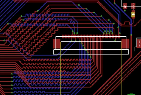
- Route Differential Pairs Properly: Keep differential pairs (common in Ethernet designs) closely coupled with equal lengths to maintain signal timing. Avoid sharp bends; use 45-degree angles or arcs for turns.
- Use Decoupling Capacitors: Place decoupling capacitors near power pins of high-speed ICs to filter noise from power planes. For a 10 Gbps switch IC, use a mix of 0.1 μF and 1 μF capacitors for effective noise suppression.
- Simulate Your Design: Before fabrication, use simulation tools to analyze signal integrity, impedance, and crosstalk. This step can identify potential issues in your network switch PCB layer stack early on.
- Follow Design Guidelines: Adhere to industry standards like IPC-2221 for PCB layout and grounding to minimize EMI and ensure reliability.
Common Mistakes to Avoid in Network Switch PCB Stack-Up Design
Even experienced designers can make errors that harm signal integrity. Here are some pitfalls to watch out for:
- Ignoring Ground Plane Continuity: Breaks in ground planes under high-speed traces can disrupt return paths, leading to EMI and signal loss.
- Neglecting Impedance Control: Failing to calculate and verify trace impedance can result in reflections, especially for signals above 1 Gbps.
- Overloading Layers: Placing too many high-speed signals on a single layer without proper spacing increases crosstalk risk.
- Poor Material Choice: Using low-cost materials with inconsistent dielectric properties can cause impedance variations in a controlled impedance PCB.
Conclusion: Building a Foundation for High-Speed Performance
Designing a network switch PCB layer stack is a critical step in achieving optimal signal integrity in network switches. By carefully selecting the number of layers, prioritizing ground planes, implementing PCB stackup impedance control, and following best practices for high-speed PCB design, you can create a robust controlled impedance PCB that supports even the most demanding network applications.
Whether you're working on a 1 Gbps switch for a small office or a 100 Gbps switch for a data center, the secrets shared in this blog provide a roadmap to success. Focus on precision in your stack-up design, collaborate with your PCB manufacturer for material and fabrication details, and always validate your design with simulations to ensure top-notch performance.
With these strategies, you’re well-equipped to tackle the challenges of modern network switch design and deliver reliable, high-speed solutions for any application.


