ALLPCB


If you're new to the world of printed circuit boards (PCBs) and looking to understand the CEM-1 PCB manufacturing process, you've come to the right place. This guide will walk you through the essentials of single-sided PCB fabrication, focusing on key steps like CEM-1 PCB etching and CEM-1 PCB drilling. Whether you're a hobbyist or a budding engineer, we'll break down the PCB manufacturing steps into simple, actionable information to help you get started with confidence.
In this comprehensive blog, we'll dive deep into each phase of creating a CEM-1 PCB, a popular material for single-sided boards due to its cost-effectiveness and reliability for simpler designs. By the end, you'll have a clear understanding of how to fabricate a PCB from scratch, with practical tips tailored for beginners. Let's get started!
What is CEM-1 Material in PCB Manufacturing?
Before we dive into the CEM-1 PCB manufacturing process, let's clarify what CEM-1 is. CEM-1 stands for Composite Epoxy Material-1, a type of base material used in PCB production. It consists of a woven glass fabric core combined with paper layers, all bonded with epoxy resin. This material is widely used for single-sided PCB fabrication because it offers a good balance of durability and affordability, making it ideal for low-cost, less complex electronic devices like calculators, toys, and basic LED lighting.
CEM-1 is not as robust as higher-grade materials like FR-4, but it still provides decent mechanical strength and electrical insulation. Its thermal resistance is moderate, typically handling temperatures up to 130°C, which is sufficient for many basic applications. Understanding this material's properties is key to mastering the manufacturing process, as it influences choices in etching, drilling, and other steps.
Why Choose CEM-1 for Single-Sided PCB Fabrication?
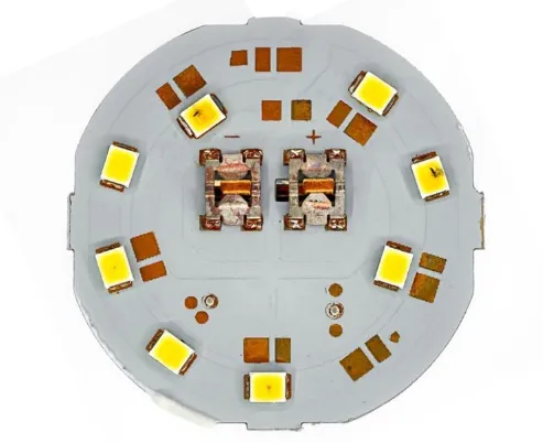
Single-sided PCBs are the simplest type of circuit boards, featuring conductive traces on only one side of the substrate. They are perfect for beginners due to their straightforward design and lower production costs. When paired with CEM-1 material, these boards become even more budget-friendly while maintaining acceptable performance for non-demanding applications.
Choosing CEM-1 for single-sided PCB fabrication also means easier handling during manufacturing. The material's composition allows for simpler CEM-1 PCB etching and CEM-1 PCB drilling processes compared to multilayer boards or higher-grade materials. This makes it an excellent starting point for those learning the ropes of PCB production.
Overview of PCB Manufacturing Steps for CEM-1 Boards
The PCB manufacturing steps for a CEM-1 single-sided board involve several key stages, each critical to ensuring the final product functions as intended. Here's a quick overview before we dive into the detailed process:
- Design and Preparation
- Material Selection and Cutting
- Imaging and Etching
- Drilling Holes
- Plating and Finishing
- Testing and Inspection
Each of these steps requires precision and attention to detail, especially when working with a material like CEM-1, which has specific handling requirements. Let's explore each phase of the CEM-1 PCB manufacturing process in depth.
Step 1: Design and Preparation for CEM-1 PCBs
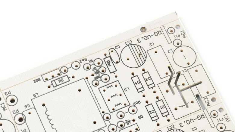
The first step in any PCB project is creating a detailed design. This involves using specialized software to draw the circuit layout, specifying where traces, pads, and components will go on the single-sided board. For beginners, the design should be kept simple to minimize errors during fabrication.
Once the design is finalized, it is transferred to a film or printed as a photomask. This mask will be used in the imaging process to define the copper traces on the CEM-1 board. Accuracy at this stage is crucial—any mistake in the design can lead to faulty connections or wasted materials. Ensure that the design file matches the board dimensions, typically measured in millimeters, such as a standard 100mm x 100mm board size for small projects.
Step 2: Material Selection and Cutting
With the design ready, the next step in the CEM-1 PCB manufacturing process is preparing the raw material. A CEM-1 laminate sheet, usually coated with a thin layer of copper on one side for single-sided boards, is selected. The thickness of the board can vary, but a common choice for beginners is 1.6mm, offering a good balance of rigidity and ease of handling.
The laminate is then cut to the required size using precision tools to match the design specifications. Clean edges are important to avoid issues during later steps like drilling or etching. Any debris or dust on the surface must be removed to ensure proper adhesion of the photoresist in the next stage.
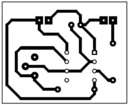
Step 3: Imaging and CEM-1 PCB Etching
Now comes one of the most critical parts of single-sided PCB fabrication: transferring the circuit pattern onto the board through imaging and CEM-1 PCB etching. A photoresist layer is applied to the copper side of the CEM-1 board. This light-sensitive coating will protect the areas of copper that form the circuit traces.
The photomask from the design stage is placed over the photoresist, and the board is exposed to UV light. The exposed areas of the photoresist harden, while the unexposed parts (covered by the mask) remain soft and are washed away with a developer solution. This reveals the copper pattern that will become the circuit.
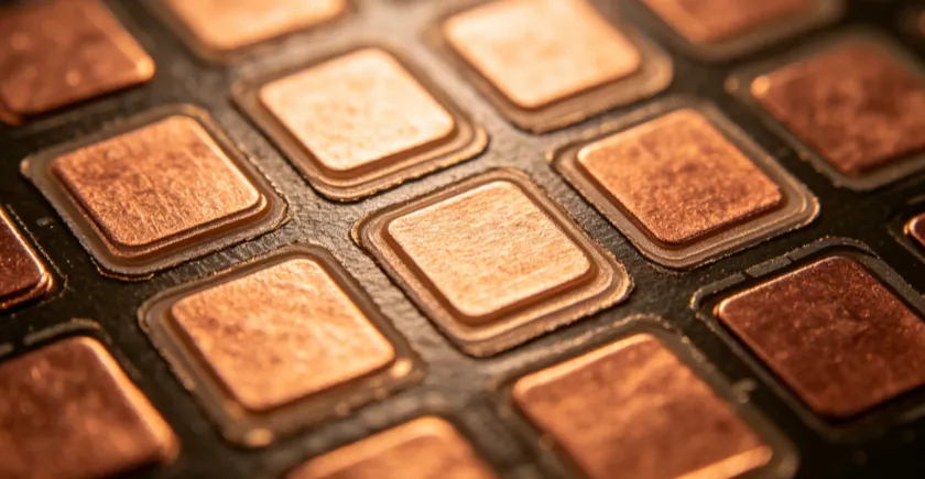
Next, the board undergoes etching, where a chemical solution, often ferric chloride, removes the unprotected copper. This process typically takes 10-30 minutes, depending on the solution's strength and the copper thickness (usually 1 oz or 35 micrometers for standard boards). After etching, the remaining photoresist is stripped off, leaving only the desired copper traces on the CEM-1 substrate.
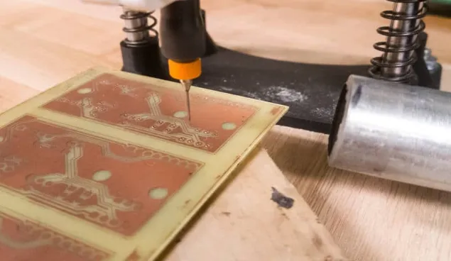
Step 4: CEM-1 PCB Drilling for Component Holes
With the circuit pattern in place, the next step in the PCB manufacturing steps is CEM-1 PCB drilling. Holes are drilled into the board to accommodate through-hole components like resistors, capacitors, and connectors. For single-sided CEM-1 PCBs, drilling is relatively straightforward since there are no internal layers to align.
Drilling is done using a CNC machine or a handheld drill for small-scale projects. The drill bit size must match the component leads, often ranging from 0.8mm to 1.2mm for common parts. Precision is key—misaligned or oversized holes can lead to poor connections or damaged components. After drilling, the board is cleaned to remove burrs and debris that could interfere with soldering.
Step 5: Plating and Surface Finishing
After drilling, the board may undergo plating if necessary, though this step is sometimes skipped in basic single-sided designs. Plating involves adding a thin layer of conductive material to the drilled holes to improve connectivity, but for many beginner projects with CEM-1, manual soldering suffices without plating.
More commonly, a surface finish is applied to protect the copper traces from oxidation and enhance solderability. A popular finish for CEM-1 PCBs is Hot Air Solder Leveling (HASL), which coats the copper with a thin layer of solder. This process ensures the board remains durable during storage and makes component attachment easier.
Step 6: Applying Solder Mask and Silkscreen
For added protection and usability, a solder mask is applied to the board. This is a thin layer of polymer that covers the copper traces, leaving only the pads exposed for soldering. It prevents accidental short circuits and protects the traces from environmental damage. For CEM-1 PCBs, a green solder mask is often used due to its visibility and cost-effectiveness.
Additionally, a silkscreen layer is printed on the board to label components, test points, and other markings. This white or black ink layer helps during assembly by indicating where each part should go, making the board user-friendly even for beginners.
Step 7: Testing and Quality Inspection
The final step in the CEM-1 PCB manufacturing process is testing and inspection. Each board is checked for defects such as incomplete traces, misaligned holes, or short circuits. A simple multimeter can be used to test continuity between traces, ensuring there are no breaks or unintended connections.
For beginners, visual inspection under good lighting can catch obvious issues like uneven etching or burrs from drilling. More advanced testing, like automated optical inspection (AOI), may be used in professional settings to ensure quality, but for small projects, manual checks are often sufficient.
Tips for Beginners in CEM-1 PCB Manufacturing
Starting with single-sided PCB fabrication using CEM-1 can be rewarding, but it comes with a learning curve. Here are some practical tips to help you succeed:
- Start Simple: Begin with basic designs to understand the process before moving to complex circuits.
- Use Proper Safety Gear: When handling chemicals for CEM-1 PCB etching, wear gloves and work in a well-ventilated area to avoid exposure to fumes.
- Double-Check Measurements: Ensure drill bit sizes and board dimensions match your design to prevent errors during CEM-1 PCB drilling.
- Practice Patience: Rushing through steps like etching or soldering can lead to mistakes. Take your time for better results.
- Invest in Quality Tools: Even for beginners, a small investment in a decent drill or etching kit can make the process smoother.
Common Challenges in CEM-1 PCB Manufacturing
While the PCB manufacturing steps for CEM-1 boards are straightforward, beginners may encounter a few hurdles. During etching, overexposure to the chemical solution can remove too much copper, weakening traces. A typical etching time of 15-20 minutes should be monitored closely. Another issue is drill bit breakage during CEM-1 PCB drilling, often due to excessive force or incorrect bit size—always start with a pilot hole if unsure.
Additionally, CEM-1's lower thermal resistance compared to other materials means it may not withstand high soldering temperatures for long. Keep soldering iron heat below 300°C and work quickly to avoid delamination or damage to the board.
Conclusion: Mastering CEM-1 PCB Fabrication
Manufacturing CEM-1 PCBs is an accessible entry point into the world of electronics for beginners. By following the detailed PCB manufacturing steps outlined in this guide—from design and CEM-1 PCB etching to CEM-1 PCB drilling and finishing—you can create functional single-sided boards for a variety of simple projects. The CEM-1 PCB manufacturing process may seem daunting at first, but with practice and attention to detail, you'll gain the skills needed to produce reliable results.
At ALLPCB, we are committed to supporting engineers and hobbyists at every stage of their PCB journey. Whether you're just starting with single-sided PCB fabrication or looking to scale up your projects, understanding the fundamentals of materials like CEM-1 is the foundation of success. Keep experimenting, stay safe, and enjoy the process of bringing your electronic ideas to life!