 ALLPCB


If you're a PCB designer looking to understand how line width in mils affects trace impedance, you're in the right place. Simply put, the width of a trace on a printed circuit board (PCB) directly impacts its characteristic impedance, which is crucial for maintaining signal integrity, especially in high-speed designs. A typical trace width of 5-10 mils might correspond to a 50-ohm impedance on a standard FR-4 material, but this varies based on factors like dielectric thickness and stack-up. In this comprehensive guide, we'll dive deep into the relationship between trace width and impedance, explore impedance control techniques, and provide practical tips for achieving controlled impedance routing in your designs.
Introduction to PCB Trace Impedance and Why It Matters
In the world of PCB design, signal integrity is everything. Whether you're working on a high-speed digital circuit or a sensitive analog application, ensuring that signals travel without distortion or interference is critical. This is where PCB trace impedance comes into play. Impedance is the opposition to the flow of alternating current in a circuit, and on a PCB, it’s determined by the physical characteristics of the trace, including its width, thickness, and the surrounding materials.
Trace impedance isn't just a theoretical concept—it directly affects how signals behave. If the impedance isn’t controlled, you might face issues like signal reflections, crosstalk, or data loss. For instance, in high-speed designs operating at frequencies above 100 MHz, mismatched impedance can lead to significant signal degradation. That’s why understanding and controlling impedance control PCB design is essential for modern electronics.

What Is Characteristic Impedance in PCB Design?
Before we dive into trace width, let’s clarify what characteristic impedance means. Characteristic impedance, often denoted as Z0, is the inherent impedance of a transmission line on a PCB. It’s the value that a signal "sees" as it travels along the trace. For many high-speed designs, a standard characteristic impedance of 50 ohms is common, though values like 75 ohms or 100 ohms are also used depending on the application.
The characteristic impedance depends on several factors, including the trace width, the thickness of the copper, the dielectric constant of the PCB material (like FR-4 with a typical dielectric constant of 4.2-4.5), and the distance to the nearest ground plane. If any of these factors change, so does the impedance. For example, a wider trace reduces impedance, while a narrower trace increases it, assuming other factors remain constant.
The Role of Trace Width in Impedance Control
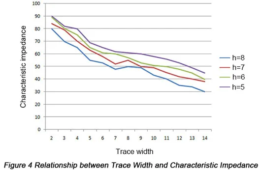
One of the most critical factors in determining trace impedance is the width of the trace, often measured in mils (1 mil = 0.001 inch). The relationship between trace width and impedance is inversely proportional: a wider trace has lower impedance, and a narrower trace has higher impedance. Why? Because a wider trace has more surface area for the signal to travel, reducing resistance and inductance per unit length.
For example, on a standard 1.6mm thick FR-4 PCB with a dielectric height of 10 mils between the trace and ground plane, a trace width of 6 mils might yield a characteristic impedance of 50 ohms. If you increase the width to 12 mils, the impedance might drop to around 35 ohms. These numbers are approximate and depend on the exact stack-up and materials, but they illustrate the principle.
Designers must carefully calculate trace widths to match the desired impedance, especially for high-speed signals where even a small mismatch can cause reflections. Tools like impedance calculators or simulation software are often used to determine the exact width needed for a specific impedance value.
Factors Affecting Trace Impedance Beyond Width
While trace width is a major factor, it’s not the only one that influences PCB trace impedance. To achieve proper impedance control PCB design, you need to consider the following:
- Dielectric Thickness: The distance between the trace and the ground plane affects impedance. A thinner dielectric layer increases capacitance, lowering impedance.
- Dielectric Constant (Er): Materials like FR-4 have a dielectric constant of around 4.2-4.5, but high-frequency designs might use materials with lower constants (e.g., 3.0) to reduce impedance variations.
- Trace Thickness: Thicker copper traces (e.g., 2 oz vs. 1 oz) slightly reduce impedance due to lower resistance.
- Trace Length and Routing: While length doesn’t directly affect characteristic impedance, long traces can introduce losses, and improper routing can cause impedance discontinuities.
Balancing these factors requires a well-thought-out PCB stack-up design. For instance, in a 4-layer board, you might place high-speed traces on the top layer with a ground plane directly below to maintain consistent impedance.
Why Controlled Impedance Routing Is Essential
Controlled impedance routing refers to designing PCB traces to maintain a specific impedance value throughout the signal path. This is crucial for high-speed applications like USB, HDMI, Ethernet, or DDR memory interfaces, where signal integrity is non-negotiable. Without controlled impedance, signals can reflect back and forth along the trace, causing errors or complete system failure.
For example, a USB 2.0 differential pair requires a differential impedance of 90 ohms. If the traces are too wide or too narrow, or if the spacing between them isn’t correct, the impedance will deviate, leading to data corruption. Controlled impedance ensures that the signal travels smoothly from source to destination without unwanted reflections.
To achieve controlled impedance, designers must specify the target impedance during the design phase and work closely with the PCB manufacturer to ensure the board is fabricated to meet those specifications. This often involves testing the impedance of sample boards using a Time Domain Reflectometer (TDR) to confirm that the traces meet the desired values.
How to Calculate Trace Width for Desired Impedance
Calculating the correct trace width for a specific impedance isn’t something you can do by guesswork. Thankfully, there are established formulas and tools to help. The most common approach is to use an impedance calculator, which takes into account the PCB stack-up, material properties, and target impedance.
For a microstrip trace (a trace on the outer layer of a PCB with a ground plane below), the characteristic impedance can be approximated using the following simplified formula:
Z0 = (87 / sqrt(Er + 1.41)) * ln(5.98 * H / (0.8 * W + T))
Where:
- Z0 = Characteristic impedance (ohms)
- Er = Dielectric constant of the material
- H = Height of the dielectric layer (mils)
- W = Trace width (mils)
- T = Trace thickness (mils)
While this formula provides a starting point, it’s often more practical to use online calculators or PCB design software with built-in impedance tools. These tools allow you to input your stack-up details and target impedance (e.g., 50 ohms) to get the required trace width in mils.
For instance, if you’re targeting a 50-ohm impedance on a 1.6mm FR-4 board with a 10-mil dielectric height, the calculator might suggest a trace width of around 6-7 mils. Always verify these calculations with your manufacturer, as fabrication tolerances can affect the final impedance.
Practical Tips for Achieving Impedance Control in PCB Design
Now that you understand the basics of trace width and impedance, here are some actionable tips to help you design PCBs with controlled impedance:
- Define Impedance Requirements Early: Before starting your layout, identify which signals require controlled impedance (e.g., high-speed data lines) and specify the target values.
- Collaborate with Your Manufacturer: Share your stack-up and impedance requirements with your PCB fabricator. They can provide feedback on material choices and fabrication limits.
- Use Consistent Trace Widths: Avoid changing trace widths unnecessarily, as this can create impedance discontinuities. If a width change is needed, taper the trace gradually.
- Maintain Proper Spacing: For differential pairs, ensure consistent spacing between traces to maintain the required differential impedance.
- Simulate Before Fabrication: Use simulation tools to model your design and predict impedance. This can help catch issues before the board is built.
Common Challenges in Impedance Control and How to Overcome Them
Even with careful planning, achieving perfect controlled impedance routing can be challenging. Here are some common issues and solutions:
- Fabrication Tolerances: Small variations in trace width or dielectric thickness during manufacturing can alter impedance. Work with a reliable manufacturer and specify tight tolerances (e.g., ±10% for impedance).
- Signal Layer Transitions: When a trace moves between layers through a via, impedance can change. Minimize via usage for high-speed signals or use back-drilling to reduce stub effects.
- Material Variations: The dielectric constant of PCB materials can vary slightly between batches. Choose high-quality materials with consistent properties for critical designs.
By anticipating these challenges and incorporating best practices into your design process, you can minimize impedance-related issues and ensure reliable performance.
Conclusion: Mastering Trace Impedance for Better PCB Designs
Understanding the relationship between line width in mils and PCB trace impedance is a fundamental skill for any PCB designer. By carefully controlling trace width, along with other factors like dielectric thickness and material properties, you can achieve the desired characteristic impedance and ensure signal integrity in your designs. Whether you're working on a simple prototype or a complex high-speed board, proper impedance control PCB techniques are key to success.
Start by using impedance calculators to determine the right trace width for your application, follow best practices for controlled impedance routing, and collaborate with your manufacturer to meet your specifications. With these steps, you’ll be well on your way to designing PCBs that perform reliably, even under the most demanding conditions.
At ALLPCB, we’re committed to supporting designers with the tools and resources needed to bring their ideas to life. By mastering trace width and impedance, you can create boards that meet the highest standards of quality and performance.


