 ALLPCB


In the fast-evolving world of medical technology, the demand for smaller, more efficient devices is higher than ever. High-Density Interconnect (HDI) PCBs are at the forefront of this revolution, especially in patient monitoring systems. These advanced circuit boards allow for the miniaturization of medical PCBs, enabling compact designs without sacrificing performance. Whether it’s for wearables or hospital equipment, HDI PCB design for patient monitoring is shaping the future of healthcare technology.
In this blog, we’ll dive deep into how HDI PCBs are transforming patient monitoring devices. We’ll explore their benefits, design considerations, applications in wearables, solutions for space constraints, cost factors, and the role of advanced technology in medical devices. Let’s uncover why HDI PCBs are the go-to solution for modern medical electronics.
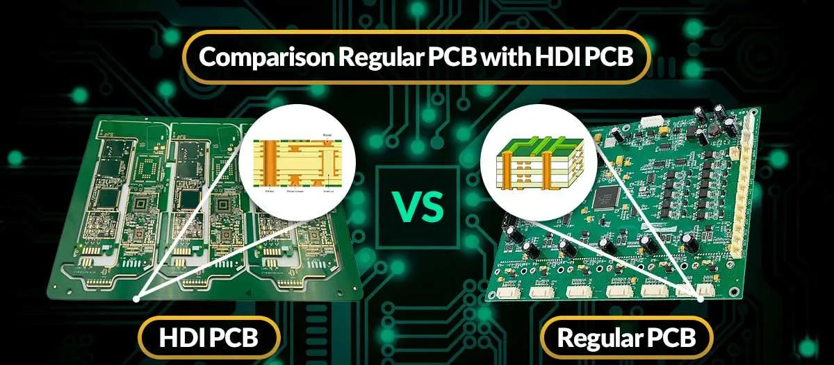
What Are HDI PCBs and Why Do They Matter for Patient Monitoring?
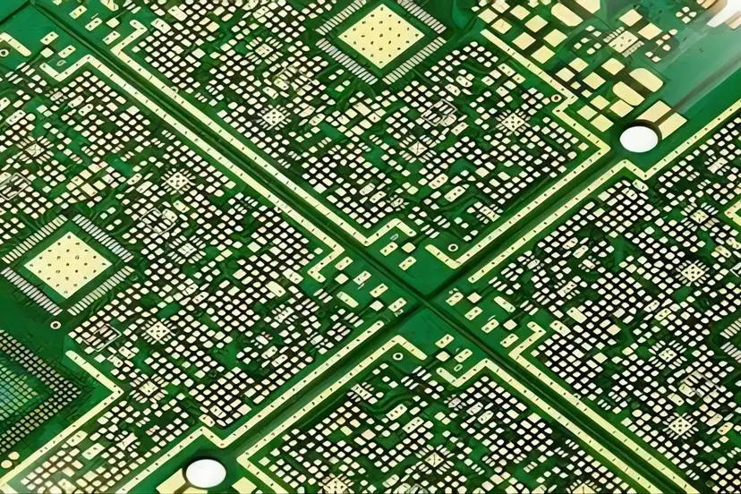
High-Density Interconnect (HDI) PCBs are a type of printed circuit board with a higher wiring density than traditional PCBs. They use microvias, fine lines, and thin materials to pack more components into a smaller space. This technology typically features line widths and spaces below 100 micrometers and via diameters as small as 50 micrometers, allowing for intricate designs in compact areas.
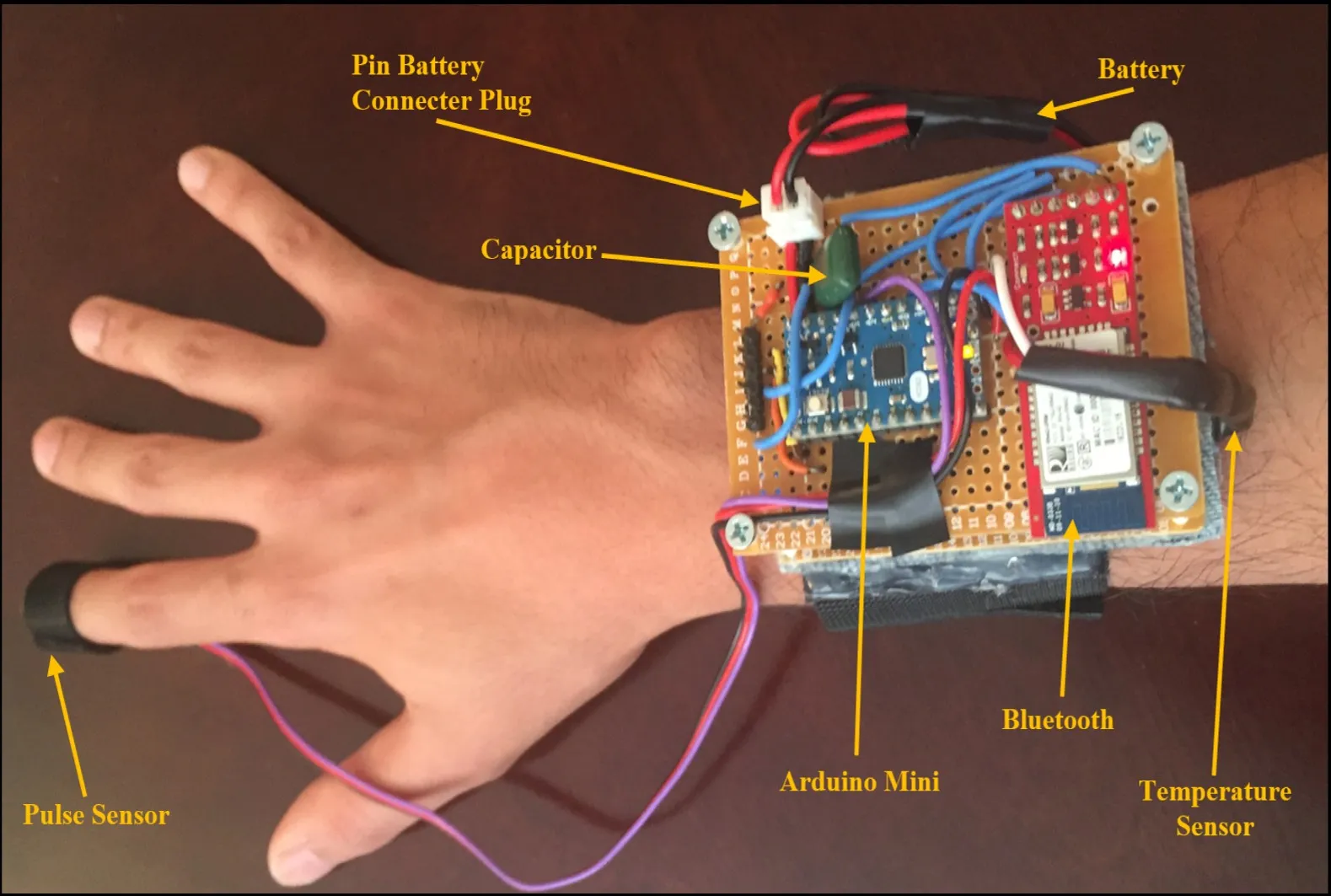
For patient monitoring devices, HDI PCBs are a game-changer. These devices, such as heart rate monitors, glucose sensors, and vital sign trackers, need to be small, lightweight, and reliable. HDI technology supports the miniaturization of medical PCBs by reducing the size of the circuitry while maintaining high performance. This means patients can wear devices comfortably for long periods, and healthcare providers can integrate more features into limited spaces.
Benefits of HDI PCB Design for Patient Monitoring
HDI PCBs offer several advantages that make them ideal for patient monitoring systems. Let’s break down the key benefits:
- Smaller Size: HDI PCBs enable significant size reduction, often up to 60% compared to standard boards. This is critical for wearable monitors that must fit comfortably on a patient’s wrist or chest.
- Higher Performance: With shorter signal paths, HDI PCBs reduce signal loss and improve speeds, ensuring accurate data transmission in real-time monitoring. For example, signal integrity can be maintained at frequencies up to 5 GHz in some designs.
- Increased Reliability: The use of microvias and advanced materials reduces the risk of failure, which is essential for life-critical medical applications.
- More Functionality: HDI technology allows for more layers (often 10 or more) in a smaller footprint, so devices can include advanced features like wireless connectivity or multiple sensors.
These benefits directly address the needs of modern healthcare, where compact, reliable, and feature-rich devices are in high demand.
Miniaturization of Medical PCBs: Solving Space Constraints
One of the biggest challenges in designing patient monitoring devices is dealing with patient monitoring PCB space constraints. Whether it’s a wearable heart monitor or a portable ECG machine, the available space for electronics is often limited. HDI PCBs tackle this issue head-on by allowing designers to stack multiple layers and use microvias instead of larger through-holes.
For instance, a typical wearable device might need to house a processor, battery, sensors, and wireless module in a space no larger than a few square centimeters. With HDI technology, designers can reduce the board size while maintaining or even increasing the number of components. This is achieved by using blind and buried vias, which save space by connecting layers internally rather than drilling through the entire board.
High-Density PCB for Wearables: A Perfect Match
Wearable medical devices, such as fitness trackers and smartwatches with health monitoring features, are becoming essential tools for both patients and healthcare providers. A high-density PCB for wearables is crucial to meet the dual demands of small size and robust functionality.
HDI PCBs enable wearables to include advanced features like continuous heart rate monitoring, blood oxygen level tracking, and even temperature sensing in a slim, lightweight form. The fine traces and high layer counts (sometimes up to 12 layers in a board less than 1 mm thick) ensure that these devices can process and transmit data efficiently. Additionally, HDI designs support flexible and rigid-flex PCBs, which are often used in wearables to conform to curved or irregular shapes.
The result is a device that patients can wear all day without discomfort, while still providing accurate, real-time data to medical professionals. This trend is driving the growth of personalized healthcare, where patients can monitor their conditions from the comfort of their homes.
Design Considerations for HDI PCBs in Patient Monitoring
While HDI PCBs offer incredible benefits, designing them for medical applications requires careful planning. Here are some critical factors to consider in HDI PCB design for patient monitoring:
- Signal Integrity: High-frequency signals in patient monitoring devices must be transmitted without interference. Designers must optimize trace widths and spacing to maintain impedance, often targeting values like 50 ohms for RF signals.
- Thermal Management: Compact designs can generate heat, especially in devices with high processing power. Using materials with high thermal conductivity and adding heat sinks can prevent overheating.
- Material Selection: Medical PCBs often require biocompatible and durable materials to ensure safety and longevity. High-Tg (glass transition temperature) materials, such as FR-4 with Tg above 170°C, are commonly used for stability under varying conditions.
- Compliance with Standards: Medical devices must meet strict regulations like ISO 13485 and IEC 60601-1. HDI PCB designs need to account for electromagnetic compatibility (EMC) and patient safety.
By addressing these factors, engineers can create HDI PCBs that meet the rigorous demands of medical applications while pushing the boundaries of miniaturization.
HDI PCB Cost Analysis: Balancing Performance and Budget
While HDI PCBs provide unmatched advantages, they often come with a higher price tag compared to traditional boards. Conducting an HDI PCB cost analysis is essential for manufacturers and designers to balance performance with budget constraints.
The cost of HDI PCBs is influenced by several factors:
- Layer Count: More layers mean higher manufacturing complexity and cost. A 10-layer HDI board can cost 2-3 times more than a 4-layer standard PCB.
- Microvia Technology: Laser-drilled microvias are precise but expensive to produce, adding to the overall cost.
- Material Quality: High-performance materials for medical applications, such as low-loss dielectrics, increase expenses but are necessary for reliability.
- Volume: Producing HDI PCBs in larger quantities can reduce the per-unit cost, making it more feasible for mass-market medical devices.
Despite the higher upfront cost, HDI PCBs often save money in the long run by reducing the need for multiple boards or larger enclosures. For patient monitoring devices, the investment in HDI technology is justified by the improved performance and patient satisfaction that compact designs bring.
Advanced PCB Technology for Medical Devices: Beyond HDI
HDI is just one part of the broader landscape of advanced PCB technology for medical devices. As patient monitoring systems become more sophisticated, other technologies are complementing HDI to push innovation further.
- Flexible and Rigid-Flex PCBs: Often combined with HDI, these boards allow for bendable designs that fit into unconventional shapes, ideal for wearables and implants.
- Embedded Components: Embedding passive components like resistors and capacitors within the PCB layers saves even more space and enhances reliability.
- 5G Integration: With the rise of telemedicine, HDI PCBs are being designed to support 5G connectivity for faster data transmission, critical for real-time monitoring over long distances.
These advancements, paired with HDI technology, are enabling the next generation of medical devices that are smaller, smarter, and more connected than ever before.
Real-World Applications of HDI PCBs in Patient Monitoring
HDI PCBs are already making a significant impact in various patient monitoring applications. Here are a few examples:
- Wearable Heart Monitors: Devices that track heart rhythms continuously use HDI PCBs to fit multiple sensors and a wireless module into a small band or patch.
- Portable Glucose Meters: For diabetic patients, compact glucose monitoring systems rely on HDI technology to integrate display, processing, and sensor components in a handheld device.
- Remote Vital Sign Trackers: Used in telemedicine, these devices transmit data like blood pressure and oxygen levels in real time, thanks to the high-density circuitry that supports advanced communication protocols.
These applications highlight how HDI PCBs are not just a technical innovation but a practical solution that improves patient outcomes and accessibility to healthcare.
Challenges and Future Outlook for HDI PCBs in Medical Technology
Despite their advantages, HDI PCBs face some challenges in the medical field. Manufacturing complexity can lead to longer lead times, and the need for specialized equipment can limit production scalability. Additionally, ensuring compliance with medical standards adds another layer of difficulty to the design process.
However, the future looks bright. Advances in manufacturing techniques, such as additive processes and automated assembly, are expected to reduce costs and improve accessibility. The global HDI PCB market is projected to grow significantly, with estimates suggesting a value of over $34 billion by 2032, driven by demand in healthcare and electronics (based on recent industry reports). This growth will likely bring more innovation to miniaturization of medical PCBs and patient monitoring solutions.
Conclusion: HDI PCBs as the Backbone of Modern Patient Monitoring
High-Density Interconnect (HDI) PCBs are revolutionizing the way we approach patient monitoring by enabling smaller, more powerful, and reliable devices. From addressing patient monitoring PCB space constraints to powering the latest high-density PCB for wearables, HDI technology is paving the way for a new era of medical innovation. While costs and design challenges remain, the benefits of improved performance and patient comfort far outweigh the hurdles.
At ALLPCB, we’re committed to supporting engineers and manufacturers in harnessing the power of HDI and advanced PCB technology for medical devices. By staying ahead of the curve, we can help bring life-saving technologies to market faster and more efficiently. Whether you’re designing a wearable monitor or a hospital-grade system, HDI PCBs are the key to unlocking the full potential of patient monitoring miniaturization.


