 ALLPCB


If you're looking to optimize your FR-4 PCB designs for signal integrity and electromagnetic compatibility (EMC), you've come to the right place. In this comprehensive guide, we'll explore the best practices for FR-4 PCB routing techniques, including differential routing, single-ended routing, ground plane routing, impedance-controlled routing, high-speed routing, EMC routing, and tips for avoiding signal reflection on FR-4 boards. Whether you're a seasoned engineer or just starting out, these actionable strategies will help you design reliable and high-performing printed circuit boards (PCBs) using FR-4 material, one of the most widely used substrates in the industry.
FR-4, a flame-retardant epoxy laminate, is a cost-effective and versatile material for PCBs, making it a popular choice for various applications. However, achieving optimal performance requires careful routing to maintain signal integrity and minimize electromagnetic interference (EMI). Let's dive into the details of how to achieve this with proven techniques tailored for FR-4 boards.
Why FR-4 PCB Routing Matters for Signal Integrity and EMC
Signal integrity refers to the quality of an electrical signal as it travels through a PCB. Poor routing can lead to issues like crosstalk, signal delay, or data loss, especially in high-speed designs. Similarly, EMC ensures that your board doesn't emit excessive EMI or get affected by external interference. FR-4, while affordable and durable, has specific dielectric properties (like a dielectric constant of around 4.2–4.5 at 1 MHz) that influence signal speed and impedance. Proper routing techniques help manage these factors to ensure your design performs as intended.
In the following sections, we'll break down specific routing methods for FR-4 PCBs to address these challenges. Each technique focuses on maintaining clean signals and meeting EMC standards, ensuring your board operates reliably in real-world conditions.
1. FR-4 PCB Differential Routing: Maintaining Signal Balance
Differential routing on FR-4 PCBs is critical for high-speed signals, such as those in USB, HDMI, or Ethernet interfaces. Differential pairs consist of two traces carrying signals of equal magnitude but opposite polarity. This setup helps cancel out noise and reduces EMI, making it ideal for high-speed data transmission.
Best Practices for FR-4 PCB Differential Routing:
- Match Trace Lengths: Keep the two traces of a differential pair as close to the same length as possible to avoid timing skew. A mismatch of even 5 mils (0.005 inches) can introduce significant delays in signals operating at 1 GHz or higher.
- Maintain Consistent Spacing: Ensure the spacing between the two traces remains constant to maintain impedance. For FR-4, a typical differential impedance target might be 90–100 ohms for USB 2.0 signals.
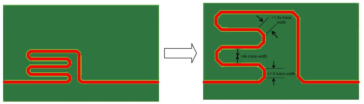
- Avoid Sharp Bends: Use 45-degree angles or smooth curves instead of 90-degree corners to prevent signal reflection on FR-4 boards.
- Route Over a Continuous Ground Plane: Place a solid ground plane beneath the differential pair to provide a stable return path and minimize EMI.
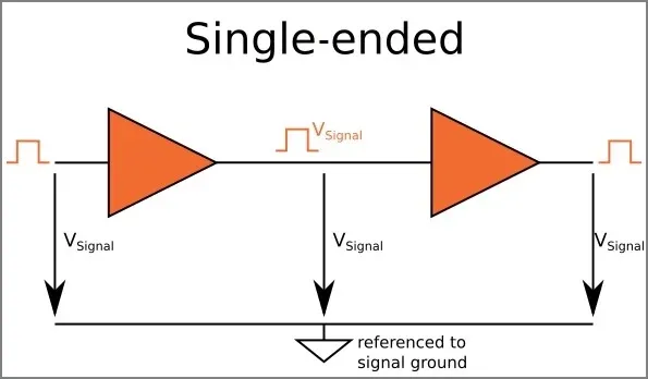
2. Single-Ended Routing on FR-4: Simplifying Low-Speed Signals
Single-ended routing on FR-4 boards is used for signals that don't require the noise immunity of differential pairs, such as low-speed digital signals or analog lines. While simpler, it still demands attention to avoid interference and maintain signal quality.
Best Practices for Single-Ended Routing on FR-4:
- Keep Traces Short: Minimize trace length to reduce the chance of noise pickup. For example, a trace longer than 10 inches on an FR-4 board can act as an antenna for EMI at frequencies above 100 MHz.
- Separate Sensitive Signals: Route analog and digital signals apart to prevent crosstalk. Maintain at least 3x the trace width as spacing between critical lines.
- Use Ground Planes: Like differential routing, ensure a continuous ground plane under single-ended traces to provide a return path and shield against interference.
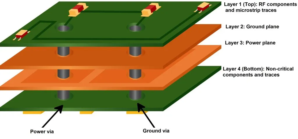
3. Ground Plane Routing on FR-4: The Foundation of Signal Integrity
A well-designed ground plane on an FR-4 PCB is essential for both signal integrity and EMC. It acts as a reference for signals, provides a low-impedance return path, and helps shield against EMI.
Best Practices for Ground Plane Routing on FR-4:
- Use Continuous Ground Planes: Avoid splitting the ground plane unless absolutely necessary, as splits can disrupt return paths and cause signal reflection on FR-4 boards.
- Place Vias Strategically: Use stitching vias to connect ground planes across layers, ensuring a low-impedance path. Space vias at intervals of λ/20 (where λ is the wavelength of the highest signal frequency) to prevent EMI leakage.
- Keep High-Speed Signals Close: Route high-speed traces directly above the ground plane to minimize loop inductance, which can be a significant issue with FR-4's dielectric properties.
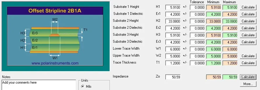
4. Impedance-Controlled Routing on FR-4: Matching for Performance
Impedance-controlled routing on FR-4 PCBs ensures that the characteristic impedance of traces matches the source and load, preventing signal reflections and maintaining integrity. FR-4's dielectric constant (around 4.2–4.5) directly impacts impedance, so precise calculations are necessary.
Best Practices for Impedance-Controlled Routing on FR-4:
- Calculate Trace Width and Spacing: Use impedance calculators or simulation tools to determine the correct trace width and spacing for your target impedance. For a 50-ohm single-ended trace on FR-4, a typical width might be 6–8 mils with a 1.6mm board thickness.
- Maintain Uniform Dielectric Thickness: Ensure consistent FR-4 layer thickness to avoid impedance variations. Variations as small as 0.1mm can alter impedance by 5% or more.
- Avoid Discontinuities: Minimize vias and layer transitions in impedance-controlled traces to prevent mismatches that cause reflections.
5. High-Speed Routing on FR-4: Managing Fast Signals
High-speed routing on FR-4 PCBs is challenging due to the material's dielectric loss and signal attenuation at frequencies above 1 GHz. Proper techniques are crucial to handle fast edge rates and maintain signal quality.
Best Practices for High-Speed Routing on FR-4:
- Minimize Trace Length: Keep high-speed traces as short as possible to reduce attenuation. For signals at 2.5 GHz, a trace longer than 2 inches on FR-4 can result in noticeable signal loss.
- Use Controlled Impedance: As discussed earlier, match the trace impedance to the system requirements to avoid reflections.
- Avoid Crosstalk: Space high-speed traces at least 3x the trace width apart to prevent interference. For differential pairs, maintain tight coupling within the pair but separate from other signals.
6. EMC Routing on FR-4: Reducing Interference
EMC routing on FR-4 focuses on minimizing EMI emissions and ensuring the board can withstand external interference. This is especially important for compliance with regulatory standards like FCC or CE.
Best Practices for EMC Routing on FR-4:
- Enclose High-Speed Signals: Route high-speed or noisy signals between ground planes or with ground shielding to contain EMI.
- Use Decoupling Capacitors: Place decoupling capacitors (e.g., 0.1 μF) near power pins to filter noise and stabilize voltage, reducing EMI on FR-4 boards.
- Avoid Loops: Minimize loop areas in power and ground traces to prevent them from acting as antennas for EMI radiation.
7. Avoiding Signal Reflection on FR-4: Preventing Signal Loss
Signal reflection on FR-4 PCBs occurs when there's an impedance mismatch along the signal path, causing part of the signal to bounce back and interfere with the original. This can degrade performance, especially in high-speed designs.
Best Practices for Avoiding Signal Reflection on FR-4:
- Match Impedance: As mentioned in impedance-controlled routing, ensure traces match the system's characteristic impedance (e.g., 50 ohms for most RF applications).
- Terminate Signals Properly: Use termination resistors at the end of long traces to absorb signals and prevent reflections. For instance, a 50-ohm resistor can terminate a 50-ohm trace effectively.
- Minimize Vias and Bends: Each via or sharp bend introduces a discontinuity that can cause reflection. Keep the signal path as smooth and direct as possible.
Conclusion: Mastering FR-4 PCB Routing for Optimal Performance
Designing an FR-4 PCB with excellent signal integrity and EMC requires attention to detail and adherence to best practices. From differential and single-ended routing to ground plane design, impedance control, high-speed routing, EMC considerations, and avoiding signal reflection, each technique plays a vital role in ensuring your board performs reliably. FR-4's unique properties, such as its dielectric constant and cost-effectiveness, make it a go-to material, but they also demand precise routing to overcome challenges like signal loss and EMI.
By applying the strategies outlined in this guide, you can create FR-4 PCB designs that meet modern performance standards while keeping costs in check. Whether you're working on a high-speed digital circuit or a mixed-signal application, these routing techniques will help you achieve a robust and efficient design.
Take the time to plan your layout, simulate impedance where possible, and follow these guidelines for differential routing, single-ended routing, and more on FR-4 boards. With careful design, your PCB will not only function as intended but also comply with EMC requirements, ensuring success in your next project.


