ALLPCB


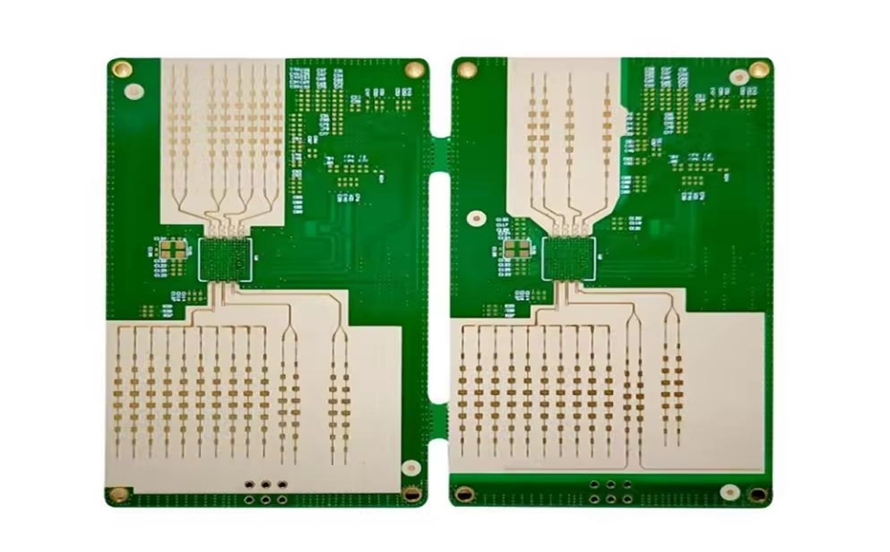
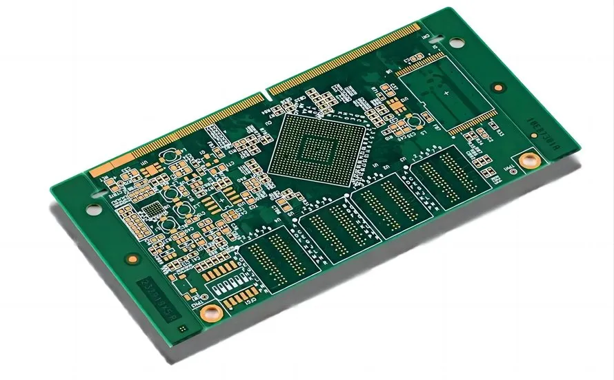
In the fast-evolving world of automotive electronics, Electronic Control Units (ECUs) are at the heart of vehicle performance, managing everything from engine control to safety systems. As ECUs become more complex, the demand for compact, high-performance printed circuit boards (PCBs) grows. One key solution to achieve this is by using blind and buried vias in High Density Interconnect (HDI) PCB designs. These advanced via technologies allow engineers to optimize PCB layout density, fitting more functionality into smaller spaces. In this blog, we’ll explore how blind vias and buried vias work, their benefits for ECU PCB design, and practical tips for implementation to achieve high density interconnect solutions.
What Are Blind and Buried Vias in PCB Design?
Before diving into their application in ECU layouts, let’s clarify what blind and buried vias are. Vias are small holes in a PCB that allow electrical connections between different layers of the board. Traditional through-hole vias go all the way through the board, but blind and buried vias offer more flexibility for dense designs.
- Blind Vias: These vias connect an outer layer of the PCB to one or more inner layers but do not go through the entire board. For example, a blind via might connect the top layer to the second layer without reaching the bottom layer. This saves space on the opposite side of the board.
- Buried Vias: These vias are completely internal, connecting two or more inner layers without reaching either the top or bottom surface. Since they don’t appear on the outer layers, they free up space for additional components or routing.
Both types of vias are essential in HDI PCB designs, where the goal is to maximize connection density while minimizing board size. For ECUs, where space constraints and performance demands are critical, these vias play a vital role.

Why Optimize PCB Layout Density for ECUs?
ECUs are the brains of modern vehicles, controlling functions like fuel injection, braking systems, and infotainment. As vehicles incorporate more advanced features—think autonomous driving or electric powertrains—ECUs must handle more signals and data in increasingly compact spaces. A dense PCB layout is crucial for several reasons:
- Space Constraints: Automotive designs often have limited room for electronics, requiring smaller, more efficient PCBs.
- Signal Integrity: Shorter signal paths in a dense layout reduce delays and interference, critical for high-speed data in ECUs. For instance, signal propagation delays can be reduced by up to 30% with optimized routing using HDI techniques.
- Cost Efficiency: Smaller boards use less material, and fewer layers can lower manufacturing costs if density is managed effectively.
Blind and buried vias help achieve this density by allowing more connections in less space, reducing the need for additional layers or larger boards.
Benefits of Blind and Buried Vias for HDI ECU PCB Design
Using blind and buried vias in ECU PCB layouts offers several advantages that directly address the challenges of high density interconnect designs. Let’s break down the key benefits:
1. Increased Routing Space
Traditional through-hole vias take up space on every layer of the PCB, even if they’re not needed on some layers. Blind and buried vias, however, only occupy space where they are necessary. This frees up room for additional traces and components, allowing for tighter routing. For example, in a 6-layer ECU PCB, using blind vias between layers 1 and 2 can leave layers 5 and 6 available for other connections.
2. Reduced Board Size
By enabling more connections in a smaller area, these vias help shrink the overall footprint of the PCB. In automotive applications, where every millimeter counts, this can make a significant difference. A study on HDI designs showed that boards using blind and buried vias could reduce area by up to 25% compared to traditional layouts.
3. Improved Signal Performance
Shorter via lengths in blind and buried configurations reduce signal loss and crosstalk, which are critical for high-speed signals in ECUs. For instance, a blind via connecting only two adjacent layers can lower impedance mismatches, maintaining signal integrity at speeds above 1 GHz, which is common in modern automotive communication protocols like CAN-FD or Ethernet.
4. Enhanced Thermal Management
Dense layouts often face heat dissipation challenges. Blind and buried vias can be strategically placed to avoid thermal hotspots, allowing better heat distribution across the board. This is vital for ECUs operating in harsh automotive environments where temperatures can exceed 85°C.
How Blind and Buried Vias Optimize ECU PCB Layout Density
Now that we understand the benefits, let’s look at how these vias specifically optimize PCB layout density for ECUs. The following points detail their role in HDI designs:
1. Layer Stacking Efficiency
In a typical ECU PCB, multiple layers are used to route power, ground, and signal traces. Blind vias allow connections between specific layers without penetrating unnecessary ones, reducing via stub effects (unused portions of vias that can cause signal reflection). For example, a blind via connecting layer 1 to layer 3 avoids creating stubs on layers 4 through 6, optimizing space and performance.
2. Component Placement Flexibility
Buried vias, being internal, don’t interfere with surface-mounted components on the top or bottom layers. This allows for denser component placement, which is essential for ECUs that often integrate microcontrollers, sensors, and communication chips in a small area.
3. Support for Microvias in HDI
Blind and buried vias are often used alongside microvias (vias with diameters less than 0.15 mm) in HDI designs. Microvias enable even finer connections, and when combined with blind and buried vias, they create a highly compact layout. For instance, a 10-layer ECU board might use microvias for fine-pitch components like BGA (Ball Grid Array) packages, while blind vias handle interlayer routing.
4. Minimized Signal Layers
By using these vias, engineers can reduce the number of signal layers needed. A design that might require 8 layers with through-hole vias could potentially be reduced to 6 layers with blind and buried vias, saving cost and space while maintaining functionality.

Practical Tips for Implementing Blind and Buried Vias in ECU Designs
While the advantages are clear, implementing blind and buried vias in HDI ECU PCB designs requires careful planning. Here are some actionable tips to ensure success:
1. Collaborate Early with Manufacturers
Blind and buried vias require advanced manufacturing techniques like laser drilling and sequential lamination. Work closely with your PCB fabrication partner to confirm their capabilities, such as minimum via sizes (often 0.1 mm for blind vias) and aspect ratios (typically 1:1 for microvias). Early collaboration helps avoid design revisions and ensures manufacturability.
2. Use Design Software for Via Planning
Modern PCB design tools allow you to define via types and simulate their impact on signal integrity. Use these tools to plan via placement, ensuring they align with component layouts and signal paths. For high-speed ECU signals, aim to keep via transitions under 0.5 mm in length to minimize inductance.
3. Balance Cost and Complexity
While blind and buried vias save space, they can increase manufacturing costs due to additional process steps. Evaluate whether the density gains justify the expense. For instance, using buried vias only in critical high-density areas can keep costs manageable.
4. Test for Reliability
Automotive ECUs must withstand vibration, temperature extremes, and humidity. Ensure that via structures are tested for reliability under these conditions. Standards like IPC-6012 for PCB qualification can guide testing protocols, targeting a via failure rate of less than 0.1% over the product lifecycle.
Challenges to Consider with Blind and Buried Vias
While these vias are powerful tools for optimizing PCB layout density, they come with certain challenges:
- Higher Manufacturing Costs: The specialized processes for creating blind and buried vias, such as laser drilling, can raise production expenses by 20-30% compared to standard through-hole vias.
- Design Complexity: Incorrect via placement can lead to signal integrity issues or manufacturing defects. For example, misaligned blind vias might cause open circuits if not drilled precisely.
- Testing Limitations: Since buried vias are internal, they are harder to inspect and test for faults after assembly. Advanced techniques like X-ray inspection may be necessary.
Despite these challenges, the benefits often outweigh the drawbacks for ECU applications where density and performance are non-negotiable.
Real-World Applications in Automotive ECUs
Blind and buried vias are already transforming ECU designs across various automotive systems. For instance, in engine control modules, HDI PCBs with these vias enable the integration of high-speed sensors and actuators in a compact form factor. In advanced driver-assistance systems (ADAS), they support the dense routing needed for processing large volumes of data from cameras and radar in real-time, often at speeds exceeding 2.5 Gbps.
Another example is in electric vehicle (EV) battery management systems, where ECUs monitor cell health and balance power distribution. Here, blind vias help reduce board size while maintaining low impedance paths for power signals, ensuring efficiency and safety.
Conclusion: The Future of ECU PCB Design with HDI
As automotive electronics continue to advance, the need for high density interconnect solutions in ECU PCB design will only grow. Blind and buried vias are essential tools for optimizing PCB layout density, offering space savings, improved signal performance, and design flexibility. By understanding their benefits and implementing them with careful planning, engineers can create compact, reliable, and high-performing ECUs that meet the demands of modern vehicles.
Whether you’re designing for engine control, safety systems, or electric vehicle applications, leveraging blind and buried vias in HDI PCB layouts can give you a competitive edge. With the right approach and collaboration with manufacturing experts, these technologies can help you push the boundaries of what’s possible in automotive electronics.