 ALLPCB


When designing a multilayer PCB, one of the most critical factors to consider is the dielectric thickness between layers. This seemingly small detail plays a huge role in ensuring signal integrity, managing power distribution, and minimizing interference. So, how do you optimize dielectric layer thickness in a multilayer PCB stackup for the best performance? The answer lies in balancing factors like impedance control, signal speed, and power plane design while selecting the right materials and layer arrangement. In this blog, we’ll dive deep into the importance of dielectric thickness, explore best practices for multilayer PCB stackup, and provide actionable tips to enhance your PCB designs for signal integrity and overall performance.
What Is Dielectric Thickness in Multilayer PCBs?
Dielectric thickness refers to the distance between conductive layers (like signal traces or power planes) in a multilayer PCB, separated by an insulating material known as the dielectric. Common dielectric materials include FR-4, a fiberglass-epoxy laminate, and other advanced materials with specific electrical properties. This thickness directly impacts how signals travel through the board, how much crosstalk occurs between traces, and how effectively power is distributed across layers.
In a multilayer PCB stackup, which typically consists of 4, 6, 8, or more layers, dielectric thickness varies depending on the design goals. For instance, a thinner dielectric layer might be used between a signal layer and a ground plane to control impedance tightly, while a thicker dielectric could be chosen between power and ground planes to reduce capacitance. Understanding and optimizing this thickness is key to achieving high performance in complex electronic designs.
Why Dielectric Thickness Matters in Multilayer PCB Stackup
The dielectric thickness in a multilayer PCB stackup isn’t just about physical separation—it’s about electrical performance. Here are the main reasons why it’s so important:
- Signal Integrity: Dielectric thickness affects the characteristic impedance of signal traces. For high-speed designs, maintaining a consistent impedance (often 50 ohms for single-ended signals) is critical to prevent signal reflections and data loss. A thinner dielectric between a signal layer and its reference plane (like ground) lowers impedance, while a thicker dielectric increases it.
- Crosstalk and EMI: Thinner dielectric layers can increase the risk of crosstalk between adjacent signal traces or layers. Proper dielectric thickness helps isolate signals and reduce electromagnetic interference (EMI).
- Power Plane Design: In power distribution, dielectric thickness between power and ground planes determines capacitance. A thinner dielectric increases capacitance, which can help with noise filtering but may also lead to unwanted coupling if not managed properly.
- Signal Speed: The dielectric constant (Dk) of the material and its thickness influence the propagation delay of signals. A lower Dk and optimized thickness can help signals travel faster, which is vital for high-frequency applications.
By carefully selecting dielectric thickness, you can fine-tune your PCB layer arrangement to meet the specific needs of your application, whether it’s a high-speed digital circuit or a power-heavy design.
Factors to Consider When Choosing Dielectric Layer Thickness
Optimizing dielectric layer thickness in a multilayer PCB stackup requires balancing several factors. Let’s break them down:
1. Impedance Control for Signal Integrity
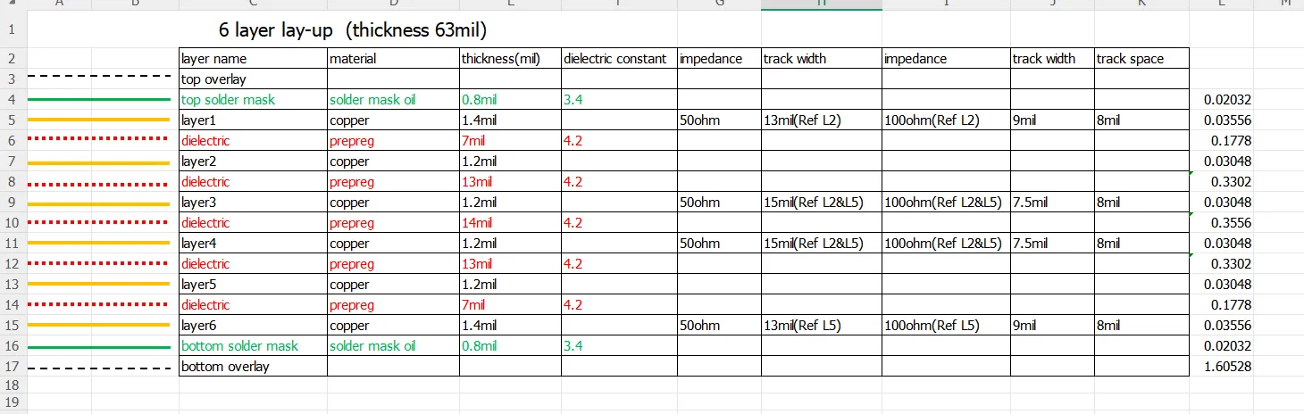
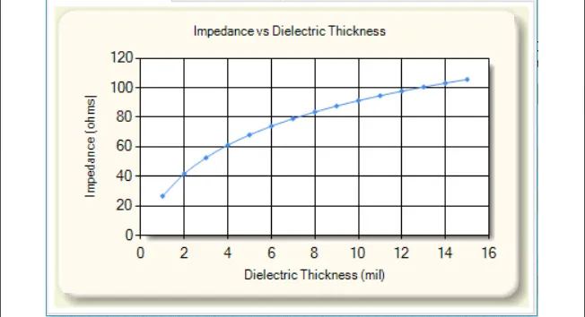
For high-speed signals, controlling impedance is non-negotiable. The dielectric thickness between a signal trace and its reference plane (usually ground) directly affects this. A common rule of thumb is to use a dielectric thickness that achieves the desired impedance based on the trace width and dielectric constant of the material. For example, with FR-4 (Dk around 4.2-4.5), a 5-mil (0.127 mm) dielectric thickness might be used for a 50-ohm impedance with a trace width of 7 mils (0.178 mm). Many design tools can simulate these values to help you choose the right thickness.
2. Layer Count and Board Thickness
The total number of layers in your multilayer PCB stackup also influences dielectric thickness. A 6-layer board might have thinner dielectrics compared to a 12-layer board to keep the overall board thickness manageable (typically 1.6 mm for standard designs). However, cramming too many layers into a thin board can lead to manufacturing challenges and signal issues. Work with your fabrication team to ensure the dielectric thickness aligns with both design and production capabilities.
3. Power Plane Capacitance
In power plane design, dielectric thickness between power and ground layers impacts interplane capacitance. A thinner dielectric (e.g., 3-5 mils or 0.076-0.127 mm) increases capacitance, which can act as a natural decoupling capacitor to filter out noise. However, if the dielectric is too thin, it might cause excessive coupling or manufacturing defects like shorts. A thicker dielectric (e.g., 10-20 mils or 0.254-0.508 mm) might be better for high-voltage designs to prevent breakdown.
4. Material Properties
The dielectric material’s properties, such as its dielectric constant (Dk) and dissipation factor (Df), interact with thickness to affect performance. Materials with a lower Dk (like some advanced laminates) allow for faster signal propagation and may require different thickness choices compared to standard FR-4. Always consider the material specs when planning your stackup.
Best Practices for Optimizing Dielectric Thickness in PCB Layer Arrangement
Now that we’ve covered why dielectric thickness matters, let’s look at actionable steps to optimize it in your multilayer PCB stackup for maximum performance.
1. Plan Your Stackup Early
Start by defining the purpose of each layer in your PCB layer arrangement. For example, in a 6-layer stackup, a common arrangement might be:
- Layer 1: Top Signal
- Layer 2: Ground Plane
- Layer 3: Inner Signal
- Layer 4: Inner Signal
- Layer 5: Power Plane
- Layer 6: Bottom Signal
Place ground planes close to signal layers with thin dielectrics (e.g., 4-6 mils or 0.1-0.15 mm) to maintain signal integrity in multilayer designs. Keep power and ground planes adjacent with a dielectric thickness that balances capacitance and isolation (e.g., 10 mils or 0.254 mm).
2. Use Simulation Tools
Modern PCB design software includes stackup editors and impedance calculators. Use these tools to test different dielectric thicknesses and materials before finalizing your design. For instance, simulating a 50-ohm trace with a 5-mil dielectric might show a perfect match, while a 10-mil dielectric could push impedance to 75 ohms, causing mismatches.
3. Minimize Crosstalk with Proper Spacing
Avoid placing high-speed signal layers too close to each other without a ground plane in between. A dielectric thickness of at least 8-10 mils (0.2-0.254 mm) between signal layers can help reduce crosstalk, especially in dense designs. If space is tight, prioritize thinner dielectrics only where impedance control is critical.
4. Collaborate with Your Manufacturer
Not all dielectric thicknesses are easy to fabricate. Standard thicknesses like 5 mils, 10 mils, or 20 mils are often readily available, but custom values might increase costs or lead times. Early collaboration with your fabrication partner ensures your multilayer PCB stackup design is manufacturable without sacrificing performance.
5. Test and Iterate
After prototyping, test your PCB for signal integrity, power stability, and EMI. Tools like oscilloscopes and network analyzers can reveal if dielectric thickness is causing issues like reflections or noise. Adjust your stackup design in subsequent iterations if needed.
Common Challenges and Solutions in Dielectric Thickness Optimization
Even with careful planning, challenges can arise when optimizing dielectric thickness. Here are some common issues and how to address them:
- Manufacturing Limitations: Very thin dielectrics (below 3 mils or 0.076 mm) can be hard to fabricate consistently. Solution: Stick to standard thicknesses or use prepreg materials that offer reliable thin layers.
- Signal Reflections: Incorrect dielectric thickness can cause impedance mismatches. Solution: Use controlled impedance design techniques and verify with simulations.
- Cost Constraints: Advanced dielectric materials or non-standard thicknesses can be expensive. Solution: Balance performance needs with budget by using standard FR-4 where high performance isn’t critical.
- Thermal Issues: Thin dielectrics in power plane designs can lead to heat buildup. Solution: Increase thickness in high-current areas or improve thermal vias and heat sinks.
Dielectric Thickness for High-Speed and High-Power Designs
Different applications have unique requirements for dielectric thickness. Let’s explore two common scenarios:
High-Speed Digital Designs
For applications like USB, HDMI, or DDR memory interfaces, signal integrity in multilayer PCBs is paramount. Dielectric thickness between signal and ground layers should be minimized (e.g., 3-5 mils or 0.076-0.127 mm) to maintain tight impedance control. Additionally, use low-loss dielectric materials with a Dk below 3.5 if possible to reduce signal delay.
High-Power Applications
In power electronics, such as motor drives or power supplies, focus on dielectric thickness between power and ground planes. A thickness of 10-20 mils (0.254-0.508 mm) often works well to provide enough isolation while still offering some capacitance for noise reduction. Ensure the material can handle high voltages without breakdown—check the dielectric strength rating (typically 20-50 kV/mm for FR-4).
Conclusion: Mastering Dielectric Thickness for Optimal PCB Performance
Dielectric thickness in multilayer PCB stackup design is a small detail with a massive impact. By carefully considering factors like impedance control, signal integrity, power plane design, and material properties, you can optimize your PCB layer arrangement for top performance. Whether you’re working on a high-speed digital board or a robust power system, the right dielectric thickness ensures signals travel cleanly, power is distributed efficiently, and interference is minimized.
Start by planning your stackup early, using simulation tools, and collaborating with your fabrication partner. Test your designs, iterate as needed, and always prioritize the specific needs of your application. With these strategies, you’ll be well on your way to creating multilayer PCBs that perform reliably under any conditions. At ALLPCB, we’re here to support your journey with expert guidance and high-quality manufacturing solutions tailored to your unique requirements.


