 ALLPCB


In high-speed PCB design, selecting the right prepreg thickness is crucial for ensuring signal integrity and minimizing signal loss. Prepreg, a key material in multilayer PCBs, acts as both an insulator and a bonding layer between copper layers. Its thickness and material properties directly impact impedance control, signal speed, and overall performance. For engineers working on high-speed applications like 5G, IoT, or data centers, understanding how to choose the optimal high-speed PCB prepreg can make or break a design.
In this comprehensive guide, we’ll dive deep into the factors that influence prepreg thickness selection, explore prepreg material properties, and explain how these choices affect signal integrity and signal loss. Whether you’re a seasoned PCB designer or new to high-speed designs, this article will provide actionable insights to help you make informed decisions.
What Is Prepreg and Why Does It Matter in High-Speed PCB Design?
Prepreg, short for "pre-impregnated," is a fiberglass fabric soaked in resin and partially cured. It’s used in multilayer PCBs to bond layers of copper foil and core materials together while providing electrical insulation. In high-speed PCB design, prepreg plays a critical role because it influences the dielectric constant (Dk) and loss tangent (Df), which affect how signals travel through the board.
In high-speed applications, where signals operate at frequencies above 1 GHz, even small variations in prepreg properties can lead to issues like signal distortion, crosstalk, or impedance mismatches. Choosing the right prepreg for signal integrity ensures that signals remain clear and reliable, even at high speeds.
Factors to Consider in Prepreg Thickness Selection for High-Speed PCBs
Selecting the right prepreg thickness isn’t a one-size-fits-all decision. Several factors must be considered to balance electrical performance, mechanical stability, and manufacturing constraints. Below are the key aspects to evaluate when choosing a high-speed PCB prepreg.
1. Impedance Control and Dielectric Thickness
In high-speed designs, controlled impedance is essential to prevent signal reflections and ensure reliable data transmission. The thickness of the prepreg layer directly affects the impedance of signal traces. For example, a thinner prepreg layer results in lower impedance for a given trace width, while a thicker layer increases impedance.
A common target impedance for high-speed signals, such as USB 3.0 or PCIe, is 50 ohms for single-ended traces or 100 ohms for differential pairs. To achieve this, designers must calculate the required prepreg thickness using tools like field solvers or impedance calculators, considering the dielectric constant (typically 3.5–4.5 for standard FR-4 prepreg). For instance, a 4-mil (0.1 mm) prepreg layer might be ideal for a 50-ohm trace with a 5-mil width on a standard FR-4 substrate.
2. Signal Speed and Propagation Delay
The thickness of prepreg also impacts signal propagation delay, which is the time it takes for a signal to travel along a trace. Thicker prepreg layers increase the distance between signal layers and ground planes, slowing down the signal due to a longer path through the dielectric. In high-speed designs, where timing is critical, a thinner prepreg (e.g., 2–3 mils) is often preferred to minimize delay.
For applications like DDR4 memory or 5G communication, where signals operate at 10 GHz or higher, even a difference of 1 mil in thickness can affect timing margins. Designers must balance thickness with other factors to optimize performance.
3. Signal Loss and Dielectric Properties
Signal loss is a major concern in high-speed PCB design, and prepreg material properties play a significant role. The loss tangent (Df) of the prepreg material determines how much signal energy is dissipated as heat. Standard FR-4 prepreg has a loss tangent of around 0.02, which can cause noticeable signal attenuation at frequencies above 5 GHz.
For high-speed designs, low-loss prepreg materials with a Df of 0.005 or lower are often recommended. Additionally, thinner prepreg layers can reduce signal loss by minimizing the amount of dielectric material the signal must pass through. However, extremely thin layers (below 2 mils) may pose manufacturing challenges and increase costs.
4. Mechanical Stability and Board Thickness
While thinner prepreg layers are often ideal for electrical performance, they can compromise the mechanical strength of the PCB. Thicker prepreg layers (e.g., 5–8 mils) provide better structural integrity, especially in boards with many layers or those subject to physical stress. Designers must strike a balance between electrical needs and mechanical reliability.
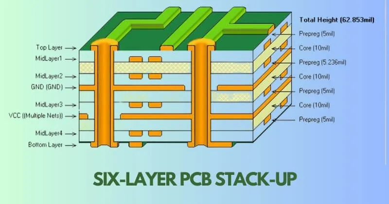
For a typical 8-layer high-speed PCB, a combination of prepreg thicknesses might be used—thinner layers (2–3 mils) near signal layers for better impedance control, and thicker layers (5–6 mils) in power or ground planes for stability.
5. Manufacturing Constraints and Cost
Not all prepreg thicknesses are readily available or cost-effective to use. Standard thicknesses like 4 mils or 6 mils are widely available and easier to process, while custom thicknesses may increase lead times and costs. Additionally, very thin prepreg layers are harder to handle during lamination, increasing the risk of defects like voids or delamination.
Consulting with your PCB manufacturer early in the design phase can help identify feasible options for prepreg thickness selection that align with both performance goals and budget constraints.
Understanding Prepreg Material Properties for Signal Integrity
Beyond thickness, the material properties of prepreg are just as important for maintaining signal integrity in high-speed designs. Let’s explore the key characteristics to consider when selecting a prepreg for signal integrity.
Dielectric Constant (Dk)
The dielectric constant, or Dk, measures how much a material slows down an electric field compared to a vacuum. In high-speed PCBs, a lower Dk value (e.g., 3.0–3.5) is preferred because it allows signals to travel faster and reduces propagation delay. Standard FR-4 prepreg has a Dk of around 4.2–4.5, which may be too high for frequencies above 10 GHz.
For ultra-high-speed applications, advanced prepreg materials with a Dk of 3.0 or lower can significantly improve performance. However, these materials often come at a higher cost, so their use should be justified by the design requirements.
Loss Tangent (Df)
As mentioned earlier, the loss tangent (Df) indicates how much signal energy is lost as heat in the dielectric material. A lower Df reduces signal loss, making it critical for high-frequency designs. For example, at 10 GHz, a prepreg with a Df of 0.003 can reduce signal attenuation by up to 50% compared to standard FR-4 with a Df of 0.02.
Low-loss prepreg materials are essential for applications like radar systems or high-speed networking equipment, where maintaining signal strength over long traces is a priority.
Thermal and Mechanical Properties
High-speed PCBs often operate in demanding environments, so prepreg materials must withstand thermal and mechanical stress. A prepreg with a high glass transition temperature (Tg), such as 170°C or above, ensures stability during soldering and operation. Additionally, the coefficient of thermal expansion (CTE) should match that of the copper and core layers to prevent warping or delamination.
How Prepreg Thickness and Material Affect Signal Loss
Signal loss in high-speed PCBs occurs due to conductor loss (resistance in copper traces) and dielectric loss (energy dissipation in the prepreg). While conductor loss can be mitigated by using wider traces or smoother copper, dielectric loss is heavily influenced by prepreg thickness and material.
Thicker prepreg layers increase dielectric loss because the signal must travel through more material, leading to higher energy dissipation. For instance, at 5 GHz, a 6-mil prepreg layer might result in 0.5 dB more loss per inch compared to a 3-mil layer of the same material. Choosing a thinner layer or a low-loss prepreg can significantly reduce this effect.
Additionally, the fiber weave effect in prepreg can contribute to signal loss and skew in differential pairs. The uneven fiberglass weave in standard prepreg can cause variations in Dk along a trace, leading to timing mismatches. Some advanced prepreg materials use a more uniform weave or non-woven glass to minimize this issue.
Best Practices for Choosing Prepreg in High-Speed PCB Design
To wrap up, here are some practical tips for selecting the right high-speed PCB prepreg for your design:
- Match Thickness to Impedance Requirements: Use impedance calculators to determine the ideal prepreg thickness for your target impedance (e.g., 50 ohms or 100 ohms).
- Prioritize Low-Loss Materials for High Frequencies: For designs above 5 GHz, opt for prepreg with a low Df (0.005 or below) to minimize signal loss.
- Balance Electrical and Mechanical Needs: Avoid overly thin layers that compromise board strength, and combine different thicknesses if needed.
- Consider Manufacturing Capabilities: Work with your PCB fabricator to select prepreg thicknesses and materials that are feasible to produce.
- Simulate Before Finalizing: Use simulation tools to model signal behavior with different prepreg options, ensuring optimal signal integrity.
Conclusion: Optimize Your High-Speed PCB with the Right Prepreg
Choosing the right prepreg thickness and material is a critical step in high-speed PCB design. By carefully considering factors like impedance control, signal speed, signal loss, and mechanical stability, you can ensure that your PCB performs reliably even at the highest frequencies. Whether you’re designing for 5G, high-speed data transfer, or advanced computing, the right prepreg for signal integrity will help you achieve your goals.


