ALLPCB


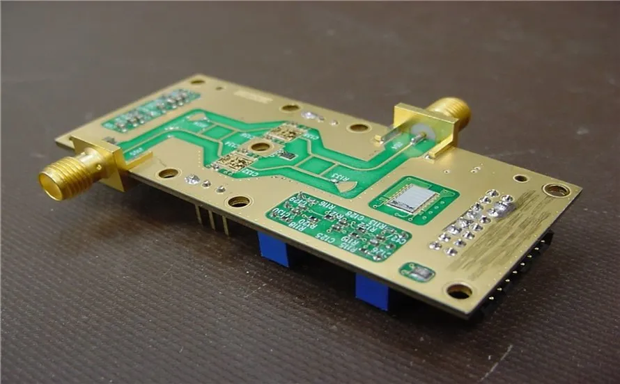
When it comes to RF PCB design, selecting the right surface finish is crucial for maintaining signal integrity and minimizing PCB signal loss, especially in high-frequency applications. The surface finish protects the copper traces, ensures proper soldering, and impacts how signals travel across the board. Choosing the wrong finish can lead to impedance mismatches, increased signal loss, and degraded performance in high-frequency PCB materials. In this comprehensive guide, we’ll explore how surface finish selection affects signal integrity and provide actionable insights to help you make informed decisions for your RF PCB projects.
Why Surface Finish Matters in RF PCB Design
In RF PCB design, every detail counts. The surface finish on a printed circuit board serves as the protective layer over the exposed copper traces, safeguarding them from oxidation and ensuring reliable connections during assembly. However, for high-frequency applications, the surface finish does more than just protect—it directly influences signal integrity and PCB impedance control. At frequencies above 1 GHz, even small variations in surface properties can cause significant signal distortions due to effects like skin depth, where signals travel primarily on the conductor’s surface.
A poorly chosen surface finish can introduce unwanted resistance, increase signal loss, and disrupt impedance matching. For example, a rough surface finish can exacerbate signal loss by increasing the effective path length for high-frequency signals. On the other hand, a well-selected finish can enhance signal transmission, reduce noise, and ensure consistent performance. Understanding these impacts is the first step to optimizing your RF PCB design for signal integrity.
Key Factors in Surface Finish Selection for Signal Integrity
Selecting the right surface finish for RF PCBs involves balancing multiple factors. Below, we break down the critical considerations that impact signal integrity, especially in high-frequency environments.
1. Surface Roughness and Signal Loss
At high frequencies, signals tend to travel along the surface of the conductor due to the skin effect. If the surface finish is rough, the signal path becomes longer and more irregular, leading to higher PCB signal loss. For instance, a surface finish with a roughness of 1.5 μm can increase signal loss by up to 20% at 10 GHz compared to a smoother finish with 0.5 μm roughness. Smoother finishes, such as Electroless Nickel Immersion Gold (ENIG), are often preferred in RF PCB design to minimize these losses.
2. Dielectric Properties and Impedance Control
PCB impedance control is vital for maintaining signal integrity in RF applications. The surface finish can indirectly affect impedance by influencing the effective dielectric constant near the conductor. Some finishes, like thick Hot Air Solder Leveling (HASL), can introduce inconsistencies in layer thickness, leading to impedance variations of up to 5 ohms in critical traces. In contrast, thinner and more uniform finishes help maintain consistent impedance, ensuring signals propagate without reflections or distortions.
3. Thermal and Mechanical Stability
High-frequency PCB materials often operate in demanding environments where thermal and mechanical stability are essential. Surface finishes must withstand temperature cycles during soldering and operation without degrading. A finish that cracks or delaminates under heat can expose copper, leading to oxidation and signal degradation. Choosing a finish with high thermal stability ensures long-term reliability for RF PCBs.
4. Corrosion Resistance and Longevity
Corrosion on the PCB surface can increase resistance and degrade signal quality over time. For RF PCBs used in harsh environments, such as telecommunications or aerospace, a corrosion-resistant finish is non-negotiable. Finishes with gold or silver layers provide excellent protection against oxidation, ensuring consistent performance over the board’s lifespan.
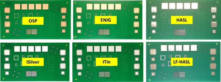
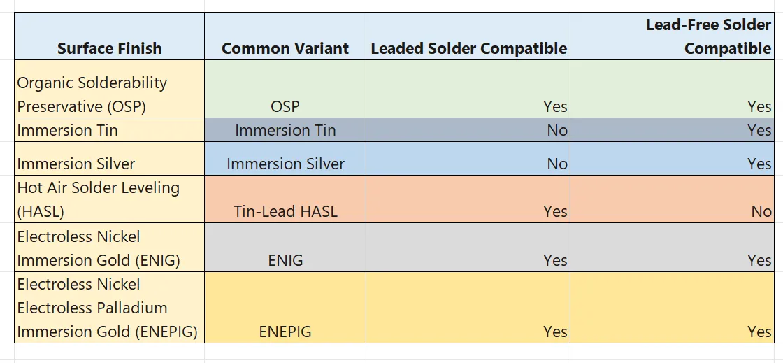
Common Surface Finishes for RF PCBs: Pros and Cons
Let’s dive into the most commonly used surface finishes for RF PCBs, evaluating their suitability for high-frequency applications and signal integrity.
1. Electroless Nickel Immersion Gold (ENIG)
ENIG is a popular choice for RF PCB design due to its smooth surface and excellent corrosion resistance. It consists of a thin layer of gold over a nickel base, providing a flat, uniform finish that minimizes signal loss. ENIG is particularly effective for maintaining PCB impedance control, with variations typically less than 1 ohm. However, it can be more expensive than other options, and the nickel layer may introduce slight magnetic losses at very high frequencies (above 20 GHz).
- Pros: Smooth surface, good solderability, long shelf life.
- Cons: Higher cost, potential magnetic losses at ultra-high frequencies.
2. Immersion Silver
Immersion Silver offers a cost-effective alternative with a smooth finish suitable for high-frequency PCB materials. It provides low signal loss and good solderability, making it a strong candidate for RF applications. However, silver is prone to tarnishing over time, which can increase resistance and affect signal integrity if not handled properly. It performs best in controlled environments, with signal loss comparable to ENIG at frequencies up to 10 GHz.
- Pros: Low cost, smooth surface, minimal signal loss.
- Cons: Susceptible to tarnishing, limited shelf life.
3. Hot Air Solder Leveling (HASL)
HASL is a traditional finish that applies a layer of solder over the copper traces. While it’s affordable and widely available, it’s not ideal for RF PCB design. The uneven surface created by HASL can increase signal loss by up to 15% at 5 GHz compared to smoother finishes. It also struggles with maintaining tight impedance control, making it less suitable for high-frequency applications.
- Pros: Low cost, widely available.
- Cons: Uneven surface, higher signal loss, poor impedance consistency.
4. Organic Solderability Preservative (OSP)
OSP is a thin organic coating that protects copper from oxidation. While it’s cost-effective and environmentally friendly, it’s not the best choice for RF PCBs. The organic layer can degrade under high temperatures, and its non-conductive nature may introduce variability in signal transmission. It’s better suited for low-frequency applications where signal integrity is less critical.
- Pros: Low cost, eco-friendly.
- Cons: Poor thermal stability, not ideal for high-frequency designs.
Matching Surface Finish with High-Frequency PCB Materials
The performance of a surface finish is closely tied to the underlying PCB material. High-frequency PCB materials, such as PTFE-based laminates or ceramic-filled substrates, have specific dielectric constants and loss tangents that influence signal behavior. For instance, a material with a dielectric constant of 2.2 (common in RF designs) requires a surface finish that minimizes additional signal loss. Pairing such materials with a smooth finish like ENIG ensures optimal performance by reducing surface-related distortions.
Additionally, the thermal expansion properties of the PCB material should align with the surface finish. Mismatched thermal expansion can lead to cracking or delamination during soldering or operation, compromising signal integrity. For example, high-frequency materials with low thermal expansion coefficients (around 10-15 ppm/°C) pair well with stable finishes to avoid mechanical stress.
Practical Tips for Surface Finish Selection in RF PCB Design
Choosing the right surface finish for your RF PCB project doesn’t have to be overwhelming. Here are some practical tips to guide your decision-making process and boost signal integrity:
- Evaluate Frequency Range: For applications above 5 GHz, prioritize smooth finishes to minimize signal loss due to skin effect. Consider options like ENIG or Immersion Silver for frequencies up to 20 GHz.
- Consider Environmental Factors: If your PCB will operate in humid or corrosive conditions, opt for a finish with high corrosion resistance to maintain long-term signal integrity.
- Balance Cost and Performance: While premium finishes offer superior performance, they come at a higher cost. Assess your project’s budget and performance requirements to find the right balance.
- Test for Impedance Control: Use simulation tools to model how different finishes affect impedance in your design. Aim for variations of less than 2 ohms for critical RF traces.
- Collaborate with Manufacturers: Work closely with your PCB fabrication partner to ensure the chosen finish is compatible with their processes and your high-frequency PCB materials.
How Surface Finish Impacts PCB Assembly and Reliability
Beyond signal integrity, the surface finish also affects the assembly process and overall reliability of the PCB. A finish with good solderability ensures strong, reliable connections during component mounting. For instance, finishes like ENIG provide a flat surface that facilitates precise soldering, reducing the risk of defects that could impact high-frequency performance.
Reliability is equally important in RF applications, where consistent performance over time is critical. A durable surface finish prevents degradation from environmental factors, ensuring the PCB maintains its signal integrity throughout its operational life. For example, a well-applied gold layer can protect against oxidation for years, preserving the board’s electrical properties.
Advanced Considerations for Ultra-High Frequency Designs
For ultra-high frequency designs operating above 20 GHz, surface finish selection becomes even more critical. At these frequencies, even minor surface imperfections can cause significant signal loss. Specialized finishes with ultra-smooth surfaces are often required to meet performance standards. Additionally, the interaction between the finish and the PCB material must be carefully analyzed to avoid parasitic effects that could disrupt signal transmission.
In such cases, advanced testing and simulation are recommended to predict how the surface finish will behave under specific conditions. Tools like electromagnetic field solvers can model signal propagation and identify potential issues before fabrication, saving time and resources.
Conclusion: Making the Right Choice for Signal Integrity
Selecting the right surface finish for RF PCB design is a critical step in ensuring signal integrity and minimizing PCB signal loss. By understanding the impact of surface roughness, dielectric properties, and environmental factors, you can make an informed decision that enhances the performance of your high-frequency PCB materials. Whether you choose a smooth and reliable option like ENIG or a cost-effective alternative like Immersion Silver, prioritizing signal integrity through careful surface finish selection will lead to better outcomes for your RF projects.
At ALLPCB, we’re committed to supporting engineers with the knowledge and resources needed to optimize their designs. By focusing on the interplay between surface finish, PCB impedance control, and high-frequency performance, you can achieve reliable, high-quality results in your next RF PCB project. Take the time to evaluate your options, test your designs, and collaborate with fabrication experts to ensure success.