 ALLPCB


In the fast-paced world of electronics, maintaining signal integrity in high-speed printed circuit boards (PCBs) is crucial. One powerful technique to achieve this is backdrilling, also known as controlled depth drilling. If you're searching for a comprehensive backdrilling design guide or specific backdrilling design rules, you're in the right place. This blog post will walk you through the essentials of controlled depth drilling design, key PCB design guidelines, and best practices for signal integrity design. Let’s dive into how backdrilling can optimize your PCB performance and ensure reliable high-speed signal transmission.
What Is Backdrilling and Why Does It Matter?
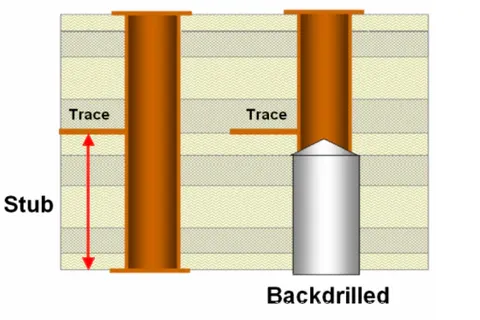
Backdrilling is a specialized manufacturing process used in PCB production to remove unused portions of copper, known as via stubs, from plated through-hole (PTH) vias. These stubs can cause signal reflections and distortions in high-speed designs, negatively impacting performance. By carefully drilling out these stubs with precision, backdrilling enhances signal integrity, making it a vital technique for modern electronics operating at data rates above 5 Gbps.
The importance of backdrilling lies in its ability to minimize signal loss and crosstalk, especially in multilayer PCBs where vias connect multiple layers. Without backdrilling, long via stubs act like antennas, introducing noise and degrading signal quality. For engineers working on high-speed applications like 5G, data centers, or telecommunications, understanding and implementing backdrilling is a game-changer.
The Basics of Controlled Depth Drilling Design
Controlled depth drilling, the core of backdrilling, involves drilling into a PCB to a precise depth to remove the unwanted copper stub without damaging the functional parts of the via. This process requires advanced machinery and careful planning during the design phase to ensure accuracy. Let’s break down the key aspects of controlled depth drilling design.
Understanding Via Stubs and Their Impact
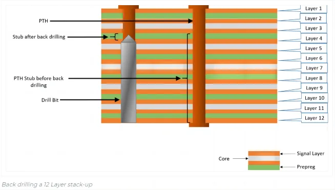
In a multilayer PCB, vias often extend beyond the layers they need to connect, creating unused copper sections called stubs. These stubs can resonate at specific frequencies, causing signal reflections. For instance, at signal speeds of 10 Gbps, a stub as short as 0.5 mm can introduce significant distortion. Backdrilling targets these stubs, reducing their length to near zero and improving signal transmission.
Precision in Depth Control
The success of backdrilling depends on controlling the drilling depth with high precision, often within tolerances of ±0.05 mm. Drilling too deep can damage the via’s functional barrel, while drilling too shallow leaves a stub that still affects signals. Modern PCB manufacturing uses advanced numerically controlled (NC) drill equipment to achieve this accuracy, often guided by design files specifying exact depths.
Backdrilling Design Rules for Success
To implement backdrilling effectively, following specific backdrilling design rules is essential. These rules ensure manufacturability and optimal performance while avoiding costly errors. Below are the critical guidelines to keep in mind during the design process.
1. Identify High-Speed Signal Vias
Not all vias in a PCB require backdrilling. Focus on vias carrying high-speed signals, typically above 3 Gbps, where signal integrity is most critical. Power and ground vias, or those used for low-speed signals, often don’t need this treatment. During the design phase, mark high-speed vias for backdrilling in your layout software to communicate intent to the manufacturer.
2. Define Stub Length Limits
Determine the maximum allowable stub length based on your signal speed. For example, at 10 Gbps, stubs should ideally be shorter than 0.2 mm to minimize reflections. Use simulation tools to analyze signal integrity and set a stub length threshold before finalizing your design.
3. Specify Drill Depths and Diameters
Backdrilling requires a slightly larger drill bit than the original via hole to remove the copper stub without affecting the via walls. Typically, the backdrill diameter is 0.15 to 0.25 mm larger than the via’s finished hole size. Clearly specify the drill depth in your design files, often as a range from the bottom layer up to just below the last connected layer.
4. Maintain Safe Clearances
Ensure that backdrilled holes don’t interfere with nearby traces or components. A minimum clearance of 0.3 mm between the backdrill edge and adjacent copper features is a common standard to prevent unintended damage during drilling.
5. Collaborate with Your Manufacturer
Backdrilling capabilities vary between manufacturers. Some can achieve tighter tolerances or handle more complex designs than others. Share your design intent early, provide detailed documentation, and confirm their ability to meet your backdrilling design rules before production begins.
PCB Design Guidelines for Signal Integrity
While backdrilling is a powerful tool, it’s just one part of a broader signal integrity design strategy. To maximize the benefits of controlled depth drilling, integrate it with other PCB design guidelines tailored for high-speed performance. Here are some essential tips to complement backdrilling.
Optimize Layer Stackup
A well-designed layer stackup minimizes the need for long vias and reduces stub lengths naturally. Place high-speed signal layers closer to the top or bottom of the board to shorten via transitions. For instance, in a 16-layer PCB, routing critical signals on layers 1 and 2 can reduce via stub length before backdrilling.
Use Ground Planes for Return Paths
Uninterrupted ground planes beneath signal traces provide a stable return path, reducing electromagnetic interference (EMI). Avoid routing high-speed signals over split planes, as this can degrade signal quality even after backdrilling.
Control Impedance
Maintain consistent trace impedance, typically 50 ohms for single-ended signals or 100 ohms for differential pairs, to prevent reflections. Use impedance calculators during design to match trace width, spacing, and dielectric thickness. Backdrilling supports this by removing stubs that could otherwise disrupt impedance.
Minimize Crosstalk
Space high-speed traces at least 3 times the trace width apart to reduce crosstalk. For differential pairs, keep traces tightly coupled and avoid routing over via stubs. Backdrilling helps by eliminating stub-related noise that could couple into nearby signals.
Benefits of Backdrilling in High-Speed Designs
Implementing backdrilling as part of your PCB design guidelines offers several advantages, especially for high-speed applications. Here’s why it’s worth the effort.
- Improved Signal Integrity: By removing via stubs, backdrilling reduces reflections and signal loss, ensuring cleaner data transmission at speeds up to 25 Gbps and beyond.
- Reduced EMI: Shorter stubs mean less radiated noise, helping your design meet electromagnetic compatibility (EMC) standards.
- Cost-Effective Solution: Compared to alternatives like blind or buried vias, backdrilling is often more affordable while delivering similar signal integrity benefits.
- Compatibility with Multilayer Boards: Backdrilling works well with complex, multilayer designs, making it a versatile choice for modern electronics.
Challenges and Limitations of Backdrilling
While backdrilling is highly effective, it’s not without challenges. Understanding these limitations helps set realistic expectations and plan accordingly.
- Manufacturing Complexity: Backdrilling adds an extra step to the fabrication process, increasing production time and cost, especially for high-density boards.
- Design Constraints: Not all vias can be backdrilled due to spacing or depth limitations. Tight designs may require alternative solutions like microvias.
- Precision Requirements: Errors in drill depth or alignment can compromise via functionality, necessitating strict quality control during manufacturing.
Best Practices for Implementing Backdrilling
To ensure success with backdrilling, follow these best practices during design and manufacturing.
- Simulate Early: Use signal integrity simulation tools to identify problematic vias and predict the impact of stubs on performance. Tools can help you prioritize which vias need backdrilling.
- Document Clearly: Include detailed notes in your design files, such as drill depth, diameter, and target vias. Clear communication prevents manufacturing errors.
- Test Prototypes: Before full-scale production, test a prototype to verify signal performance and confirm that backdrilling meets your expectations.
- Stay Updated on Standards: Follow industry standards like IPC-6012 for PCB fabrication to ensure your backdrilling design aligns with accepted practices.
Conclusion: Elevate Your PCB Design with Backdrilling
Backdrilling, or controlled depth drilling, is a proven technique for enhancing signal integrity in high-speed PCB designs. By following this backdrilling design guide and adhering to key backdrilling design rules, you can tackle the challenges of via stubs and achieve optimal performance. Pairing backdrilling with solid PCB design guidelines and signal integrity design practices ensures your boards meet the demands of modern applications, from 5G to high-performance computing.
Whether you’re designing for data rates of 10 Gbps or pushing beyond 25 Gbps, mastering controlled depth drilling design gives you a competitive edge. Take the time to plan, simulate, and collaborate with your manufacturing partner to make backdrilling a seamless part of your workflow. With these strategies, your PCBs will deliver reliable, high-quality performance every time.


