 ALLPCB


In the fast-paced world of electronics, ensuring signal integrity in high-speed printed circuit boards (PCBs) is more critical than ever. One advanced technique that addresses this challenge is the PCB back drilling process, also known as controlled depth drilling. But what exactly is back drilling, and why is it so important in modern PCB manufacturing techniques? In short, back drilling removes unused portions of via stubs in through-hole vias, reducing signal distortion and enhancing performance in high-speed designs. This blog dives deep into the intricacies of back drilling, exploring its advantages, equipment costs, and the via stub removal process to help engineers and manufacturers optimize their designs.
Whether you're an engineer looking to improve signal quality or a manufacturer aiming to refine your production process, this guide will walk you through everything you need to know about controlled depth drilling. Let’s explore how this technique is transforming PCB manufacturing and why it’s a game-changer for high-speed applications.
What Is Back Drilling in PCB Manufacturing?
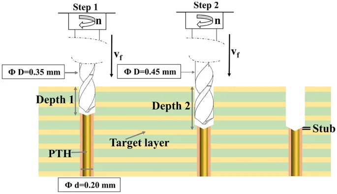
Back drilling, often referred to as controlled depth drilling, is a specialized manufacturing technique used in multilayer PCBs to remove the unused portion of a plated-through-hole (PTH) via, known as a via stub. A via stub is the leftover copper barrel in a through-hole that isn’t part of the active signal path. While vias are essential for connecting different layers in a PCB, these stubs can cause signal integrity issues, especially in high-speed designs operating at frequencies above 1 GHz.
The back drilling process involves using a drill with a slightly larger diameter than the original via hole to remove the excess copper stub from the bottom side of the PCB. This is done with precision to ensure that only the unnecessary portion is removed without damaging the functional part of the via. By eliminating these stubs, back drilling minimizes signal reflections, crosstalk, and other distortions that degrade performance.
Why Is the PCB Back Drilling Process Necessary?
In high-speed PCB designs, signal integrity is paramount. When a signal travels through a via, any unused portion of the via (the stub) acts as an antenna, causing reflections that interfere with the signal. These reflections can lead to data errors, increased noise, and reduced overall performance. For instance, in designs supporting data rates of 10 Gbps or higher, even a small stub measuring 0.010 inches can cause significant signal degradation due to impedance mismatches.
Back drilling addresses this issue by physically removing the stub, ensuring that the signal path remains clean and efficient. This process is particularly crucial for industries like telecommunications, aerospace, and data centers, where high-frequency signals and minimal latency are non-negotiable. Without back drilling, achieving the required signal quality in these applications would be nearly impossible.
Controlled Depth Drilling Advantages in PCB Design
The benefits of controlled depth drilling extend beyond just signal integrity. Here are some of the key advantages that make this technique a go-to solution in modern PCB manufacturing:
- Improved Signal Integrity: By removing via stubs, back drilling reduces signal reflections and crosstalk, ensuring cleaner transmission at high frequencies. This can lower bit error rates (BER) in digital systems, often improving performance by up to 20% in critical applications.
- Support for High-Speed Designs: As data rates climb beyond 25 Gbps in applications like 5G and advanced computing, back drilling becomes essential to meet stringent performance standards.
- Reduced Electromagnetic Interference (EMI): Via stubs can act as unintended radiators of EMI. Removing them minimizes interference, which is vital for compliance with regulatory standards.
- Cost-Effective Alternative to Blind Vias: While blind and buried vias also eliminate stubs, they are more expensive to manufacture. Back drilling offers a more budget-friendly solution for achieving similar results in many designs.
- Enhanced Design Flexibility: With back drilling, engineers can use through-hole vias without worrying about stub-related issues, simplifying layer transitions and routing in complex multilayer boards.
Understanding the Via Stub Removal Process
The via stub removal process is a precise operation that requires advanced equipment and meticulous planning. Here’s a step-by-step breakdown of how it works in PCB manufacturing:
- Design Planning: During the PCB design phase, engineers identify which vias require back drilling based on signal paths and layer connections. This is often done using simulation tools to predict stub effects on signal integrity.
- Initial Drilling and Plating: The PCB undergoes standard drilling and plating to create through-hole vias. At this stage, the vias extend through all layers of the board, creating stubs.
- Back Drilling Execution: A specialized drill, slightly larger than the original via (typically by 0.002 to 0.004 inches), is used to remove the stub from the non-functional side of the via. The drilling depth is tightly controlled to avoid damaging the active signal layers.
- Inspection and Testing: After back drilling, the PCB is inspected using techniques like X-ray imaging to ensure the stub has been removed without affecting the via’s integrity. Electrical testing confirms signal performance.
This process demands high precision, as even a slight over-drill can sever critical connections, while under-drilling can leave residual stubs that compromise signal quality. Modern manufacturing facilities use automated systems to achieve depth tolerances as tight as ±0.002 inches.
Back Drilling Equipment Cost: What to Expect
Implementing back drilling in PCB manufacturing requires investment in specialized equipment and skilled operators, which can influence overall production costs. The cost of back drilling equipment varies widely based on the complexity of the system and the volume of production. Here’s a general overview of the factors affecting back drilling equipment cost:
- CNC Drilling Machines: High-precision computer numerical control (CNC) machines capable of controlled depth drilling can range from $50,000 to over $200,000, depending on features like automated depth control and multi-spindle capabilities.
- Drill Bits and Tooling: Specialized drill bits for back drilling are more expensive than standard bits due to their precision requirements. Costs can range from $10 to $50 per bit, with frequent replacements needed for high-volume production.
- Software and Simulation Tools: Advanced design and simulation software to plan back drilling can cost between $5,000 and $20,000 annually for licenses, aiding in accurate stub identification and depth calculation.
- Labor and Training: Skilled technicians are essential for operating back drilling equipment and ensuring quality. Training programs and labor costs can add several thousand dollars per year to the budget.
While these costs may seem high, the return on investment comes from improved product reliability and reduced rework or failures in high-speed applications. For smaller manufacturers, partnering with a capable PCB fabrication service can be a cost-effective way to access back drilling without the upfront equipment expense.
PCB Manufacturing Techniques: Where Back Drilling Fits In
Back drilling is just one of many PCB manufacturing techniques used to optimize performance, but it plays a unique role in high-speed design. Unlike other methods like sequential lamination or laser drilling for microvias, back drilling specifically targets via stub issues in through-hole designs. It integrates seamlessly into the broader manufacturing workflow, typically occurring after initial drilling and plating but before final finishing processes like solder mask application.
In multilayer boards with 12 or more layers, back drilling is often combined with other techniques to achieve optimal results. For example, it may be used alongside impedance-controlled routing to ensure consistent signal performance across all layers. Manufacturers must carefully coordinate back drilling with other steps to avoid alignment issues or damage to the board’s structure.
Additionally, back drilling is a preferred choice when balancing cost and performance. While advanced via types like blind or buried vias eliminate stubs by design, their fabrication is complex and costly, often increasing production expenses by 30-50%. Back drilling provides a practical middle ground for many designs, delivering high performance without breaking the budget.
Challenges and Limitations of Back Drilling
While back drilling offers significant benefits, it’s not without challenges. Understanding these limitations can help engineers and manufacturers make informed decisions about when and how to use this technique.
- Precision Requirements: Achieving the exact drilling depth is critical. Deviations as small as 0.001 inches can either leave residual stubs or damage functional via portions, leading to costly rework.
- Increased Manufacturing Time: Back drilling adds an extra step to the production process, which can extend lead times, especially for complex boards with hundreds of vias requiring stub removal.
- Not Suitable for All Designs: Back drilling is most effective for through-hole vias in multilayer boards. It’s not applicable to surface-mount designs or boards using exclusively blind or buried vias.
- Cost Implications: Although cheaper than some alternatives, back drilling still increases manufacturing costs compared to standard through-hole designs without stub removal.
Despite these challenges, advancements in drilling technology and automation are continually reducing these drawbacks, making back drilling more accessible and efficient for a wider range of applications.
Best Practices for Implementing Back Drilling in Your Designs
To maximize the benefits of back drilling, engineers and manufacturers should follow these best practices during the design and production phases:
- Simulate Signal Performance: Use simulation software to identify vias with significant stub effects before manufacturing. Focus back drilling efforts on high-speed signal paths to optimize cost and time.
- Specify Depth Tolerances: Clearly define the required drilling depth and tolerances in your design files to avoid errors during fabrication. Typical tolerances range from ±0.002 to ±0.005 inches, depending on board thickness.
- Collaborate with Fabricators: Work closely with your manufacturing partner to ensure their equipment and processes align with your design needs. Provide detailed documentation to avoid miscommunication.
- Test and Validate: After fabrication, conduct thorough electrical testing and visual inspections to confirm that back drilling has achieved the desired results without compromising via integrity.
By adhering to these guidelines, you can ensure that back drilling enhances your PCB’s performance without introducing unnecessary risks or delays.
Conclusion: The Future of Back Drilling in PCB Manufacturing
As the demand for faster, more reliable electronics continues to grow, techniques like back drilling will remain a cornerstone of high-speed PCB manufacturing. The PCB back drilling process, with its ability to improve signal integrity through precise via stub removal, offers a practical and effective solution for modern design challenges. While the costs of back drilling equipment and the complexities of controlled depth drilling require careful consideration, the advantages in performance and reliability often outweigh these hurdles.
Whether you’re designing cutting-edge telecommunications equipment or high-performance computing systems, understanding and leveraging back drilling can give your products a competitive edge. By integrating this technique into your PCB manufacturing techniques, you’re not just solving today’s signal integrity issues—you’re preparing for the even faster, more demanding technologies of tomorrow.
At ALLPCB, we’re committed to supporting engineers and manufacturers with advanced fabrication solutions tailored to high-speed design needs. With expertise in controlled depth drilling and a focus on quality, we’re here to help bring your innovative designs to life with precision and efficiency.


