 ALLPCB


Designing a 10-layer PCB comes with unique challenges, especially when it comes to thermal management. As electronic devices become more compact and powerful, heat dissipation becomes critical to ensure reliability and performance in high-density boards. So, how do you keep a 10-layer PCB cool? The answer lies in strategic thermal management techniques like using thermal vias, optimizing layer stackup, and conducting thorough thermal analysis. In this blog, we’ll dive deep into practical solutions for 10-layer PCB heat dissipation, thermal vias, and thermal analysis to help you design boards that stay cool under pressure.
Why Thermal Management Matters for 10-Layer PCBs
10-layer PCBs are often used in complex, high-performance applications like telecommunications, medical devices, and aerospace systems. With multiple layers packed into a small space, these boards house numerous components and high-speed signals, generating significant heat. Without proper thermal management, excessive heat can lead to component failure, reduced lifespan, and degraded performance. Effective heat dissipation ensures that your board operates within safe temperature limits, maintaining reliability even under heavy loads.
In the following sections, we’ll explore proven strategies tailored for 10-layer PCB thermal management. From layout design to material selection, these tips will help you tackle heat-related challenges head-on.
Understanding Heat Sources in 10-Layer PCBs
Before diving into solutions, it’s important to identify the primary sources of heat in a 10-layer PCB. High-power components like processors, power regulators, and amplifiers generate significant heat during operation. Additionally, densely packed traces and vias can create thermal hotspots, especially in areas with high current flow. The limited space for airflow in multilayer designs further complicates heat dissipation.
For instance, a power regulator operating at 5A with a voltage drop of 2V can dissipate 10W of heat. If this heat isn’t managed, the local temperature can rise above 100°C, exceeding the safe operating range of most components (typically 85°C to 105°C). Recognizing these heat sources allows you to target specific areas for thermal management during the design phase.
Key Techniques for 10-Layer PCB Heat Dissipation
Let’s explore actionable strategies to manage heat in your 10-layer PCB designs. These methods focus on dissipating heat efficiently while maintaining signal integrity and board reliability.
1. Optimize Layer Stackup for Heat Distribution
The layer stackup in a 10-layer PCB plays a crucial role in thermal management. By dedicating specific layers to ground or power planes, you can create large copper areas that act as heat sinks, spreading heat across the board. For example, placing a ground plane near the top layer (close to heat-generating components) allows heat to transfer away from critical areas.
A typical 10-layer stackup might include multiple ground planes (e.g., layers 2, 5, and 8) to maximize heat distribution. Copper thickness also matters—using 2 oz copper instead of 1 oz can improve thermal conductivity by nearly 50%, reducing temperature rise in high-current areas.
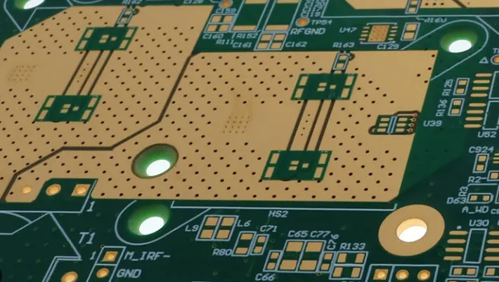
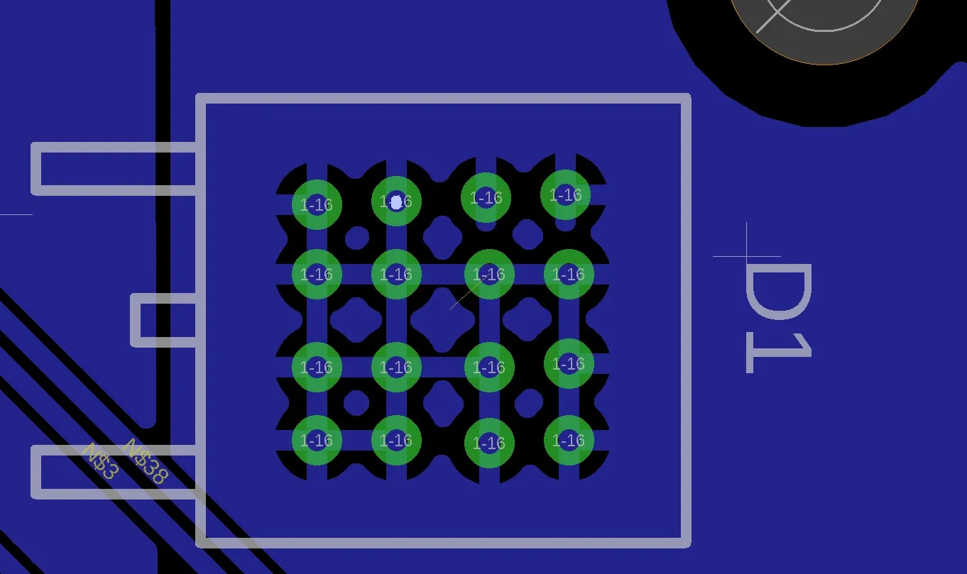
2. Use Thermal Vias for Efficient Heat Transfer
One of the most effective solutions for 10-layer PCB thermal vias is incorporating them strategically near heat-generating components. Thermal vias are small plated holes that connect heat from the top layer to internal or bottom layers, where it can dissipate into a larger copper plane or external heat sink. They create a low-resistance path for heat to escape, significantly lowering component temperatures.
For optimal results, place thermal vias in an array (e.g., a 3x3 grid) directly under high-power components. A via diameter of 0.3mm with a pitch of 1.2mm is often recommended for balancing heat transfer and manufacturability. Studies show that thermal vias can reduce junction temperatures by up to 20°C in densely packed designs, making them indispensable for 10-layer PCB heat dissipation.
3. Select Materials with High Thermal Conductivity
The choice of materials in a 10-layer PCB directly impacts its thermal performance. Standard FR-4 material has a thermal conductivity of about 0.25 W/m·K, which is insufficient for high-power designs. Consider using high-thermal-conductivity laminates, such as those with a rating of 1.0 W/m·K or higher, to improve heat dissipation.
Additionally, metal-core PCBs (MCPCBs) with an aluminum or copper base can be used for extreme cases. These materials can achieve thermal conductivities of 100-200 W/m·K, making them ideal for applications where heat dissipation is a top priority. While these materials may increase costs, they are worth the investment for maintaining performance in high-density 10-layer designs.
4. Maximize Copper Coverage in Layout Design
Increasing copper coverage on outer and inner layers helps spread heat evenly across the board. For example, fill unused areas of the PCB with copper pours connected to ground planes. This not only aids in 10-layer PCB heat dissipation but also improves electromagnetic compatibility (EMC) by reducing noise.
Ensure that copper pours are thermally connected to heat sinks or thermal vias for maximum effect. A design with 70% copper coverage on the top layer can reduce thermal resistance by up to 30% compared to a sparsely filled layout.
Conducting 10-Layer PCB Thermal Analysis
Designing for thermal management isn’t complete without proper analysis. 10-layer PCB thermal analysis involves simulating and measuring temperature distribution to identify hotspots and validate design choices. Here’s how to approach it effectively.
1. Use Thermal Simulation Software
Thermal simulation tools allow you to model heat flow in your 10-layer PCB before manufacturing. These tools calculate temperature rises based on component power dissipation, material properties, and ambient conditions. For instance, a simulation might reveal that a specific area near a high-power IC reaches 110°C, prompting you to add more thermal vias or adjust the layout.
Common simulation parameters include a power dissipation of 5-10W for high-power components and an ambient temperature of 25°C. By iterating designs in simulation, you can reduce prototyping costs and ensure your board stays within safe temperature limits (e.g., below 85°C for most components).
2. Perform Real-World Thermal Testing
Once your PCB is manufactured, conduct real-world testing using thermal imaging cameras or thermocouples. Place sensors at critical points to measure temperature under operating conditions. For example, if a component’s datasheet specifies a maximum junction temperature of 125°C, ensure the measured temperature stays at least 10-15°C below this limit to account for variations.
Testing under worst-case scenarios (e.g., maximum load at 40°C ambient temperature) helps validate your 10-layer PCB thermal analysis and uncover any design flaws. If hotspots are detected, revisit your layout to add more vias or improve airflow around the board.
Advanced Strategies for 10-Layer PCB Thermal Management
For particularly demanding applications, consider these advanced techniques to further enhance heat dissipation in your 10-layer PCB designs.
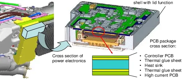
1. Integrate Heat Sinks and Thermal Pads
Attaching heat sinks to high-power components provides an external path for heat to escape. Use thermal interface materials (TIMs) like thermal pads or grease with a conductivity of 3-5 W/m·K to ensure efficient heat transfer between the component and heat sink. For a 10-layer PCB, position heat sinks on the top or bottom layer, connected via thermal vias to internal planes for maximum effect.
2. Design for Airflow and Enclosure Cooling
If your PCB is housed in an enclosure, ensure there’s adequate airflow to prevent heat buildup. Strategically place vents or fans to direct cool air over the board. For example, a small fan providing 10 cubic feet per minute (CFM) of airflow can lower board temperatures by 15-20°C in enclosed systems. In a 10-layer PCB, position high-heat components near airflow paths to maximize cooling.
3. Consider Active Cooling for Extreme Cases
In rare cases where passive cooling isn’t enough, active cooling solutions like Peltier coolers or liquid cooling systems may be necessary. These are typically used in high-performance computing or industrial applications where heat loads exceed 50W per component. While complex and costly, active cooling can maintain temperatures below 60°C even in the most demanding environments.
Common Pitfalls to Avoid in 10-Layer PCB Thermal Management
Even with the best intentions, mistakes in thermal design can lead to overheating. Here are some common pitfalls to watch out for:
- Ignoring Thermal Via Placement: Placing thermal vias too far from heat sources reduces their effectiveness. Always position them directly under or near hot components.
- Overloading Inner Layers: Avoid routing high-current traces on inner layers without adequate copper thickness, as heat can become trapped inside the board.
- Neglecting Ambient Conditions: Designs that work in a 25°C lab may fail in a 40°C industrial setting. Always account for real-world operating conditions during 10-layer PCB thermal analysis.
Conclusion: Building Cooler, More Reliable 10-Layer PCBs
Thermal management is a critical aspect of designing high-density 10-layer PCBs. By leveraging techniques like thermal vias, optimized layer stackups, and thorough thermal analysis, you can ensure effective 10-layer PCB heat dissipation and prevent overheating. Start with a solid understanding of your heat sources, use simulation tools to refine your design, and test under real-world conditions to validate performance.
Whether you’re working on telecommunications equipment or advanced medical devices, these strategies will help you keep your 10-layer PCB cool and reliable. With careful planning and attention to detail, you can tackle the thermal challenges of multilayer designs and achieve long-lasting, high-performance results.


