 ALLPCB


Component placement plays a pivotal role in ensuring the manufacturability of a printed circuit board (PCB). By following Design for Manufacturability (DFM) principles, you can optimize your PCB layout to avoid production issues, reduce costs, and improve reliability. In this comprehensive guide, we’ll explore how DFM component placement affects PCB manufacturability, dive into key guidelines like component spacing rules, and discuss strategies for pick and place optimization and solderability. Whether you’re a seasoned engineer or a beginner, this post will equip you with actionable insights to enhance your PCB designs.
What Is DFM and Why Does Component Placement Matter?
Design for Manufacturability (DFM) is a set of guidelines and practices aimed at making a PCB design easier and more cost-effective to produce. When applied to component placement, DFM ensures that parts are arranged in a way that minimizes errors during assembly, reduces manufacturing time, and enhances the overall quality of the board.
Component placement directly impacts several critical aspects of PCB production, including automated assembly (pick and place), soldering processes, and even the board’s performance in terms of signal integrity and thermal management. Poor placement can lead to issues like insufficient spacing for soldering, misalignment during assembly, or even complete production failures. By prioritizing DFM component placement, you can avoid costly redesigns and delays.
Key PCB Manufacturability Guidelines for Component Placement
To achieve a manufacturable PCB design, following specific guidelines for component placement is essential. These rules are rooted in DFM principles and address common challenges during production. Let’s break down the most important guidelines.
1. Follow Component Spacing Rules
One of the most critical aspects of DFM component placement is maintaining proper spacing between components. Insufficient spacing can lead to soldering defects, such as bridging, where solder connects adjacent pads unintentionally. It can also hinder the operation of pick and place machines, which require clear access to each component.
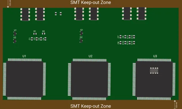
- Minimum Spacing Standards: For surface-mount components, a general rule is to maintain at least 0.2 mm (8 mils) between components to prevent soldering issues. For larger components or those with heat dissipation needs, spacing might need to be increased to 1-2 mm (40-80 mils).
- Edge Clearance: Keep components at least 3 mm (120 mils) away from the board’s edges to avoid damage during handling or panelization.
- Height Considerations: When placing tall components next to shorter ones, ensure a clearance of at least 0.5 mm (20 mils) to prevent shadowing during soldering processes like wave soldering.
Proper spacing not only aids in assembly but also improves inspection and rework processes, ensuring that any issues can be addressed without damaging nearby components.
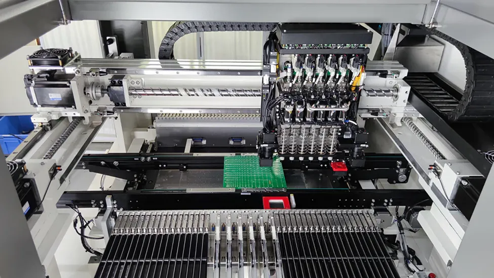
2. Optimize for Pick and Place Machines
Pick and place optimization is a cornerstone of DFM component placement. Automated assembly machines rely on precise positioning and orientation to place components quickly and accurately. If components are placed without considering these machines’ limitations, the assembly process can slow down or result in errors.
- Orientation Consistency: Align components in the same direction whenever possible, especially for polarized components like diodes and capacitors. This reduces the need for machine head rotation, speeding up the assembly process by up to 20% in some cases.
- Grid Alignment: Place components on a grid with standardized spacing (e.g., 0.1-inch or 2.54 mm increments) to simplify programming for pick and place machines.
- Fiducial Markers: Include fiducial markers near the corners of the PCB to help machines accurately locate component positions. A typical fiducial is a 1 mm diameter circle with a 2 mm clearance zone around it.
By designing with pick and place optimization in mind, you can significantly reduce assembly time and minimize the risk of misplaced components.
3. Enhance Solderability with Strategic Component Placement
Solderability is another critical factor influenced by component placement. Proper positioning ensures that solder joints are formed correctly during reflow or wave soldering, reducing defects like cold joints or tombstoning (where components lift off one pad during soldering).
- Thermal Balance: Avoid clustering high-heat-generating components in one area. Distribute them across the board to prevent uneven heating during soldering, which can cause thermal stress or warping. For example, placing power resistors or ICs with high thermal output at least 5 mm (200 mils) apart can help maintain thermal balance.
- Pad Accessibility: Ensure that solder pads are not obstructed by nearby components. For through-hole components, maintain a clearance of at least 1 mm (40 mils) around pads for manual or wave soldering.
- Component Orientation for Reflow: Orient components to minimize shadowing effects during reflow soldering. For instance, place smaller components away from the leading edge of taller ones to ensure even heat distribution.
By focusing on solderability in component placement, you can achieve stronger, more reliable connections and reduce post-assembly rework by as much as 15%, based on industry studies.
The Broader Impact of DFM Component Placement on PCB Production
Beyond the immediate benefits of following PCB manufacturability guidelines, DFM component placement has a broader impact on the entire production process. Let’s explore how it influences cost, time, and quality.
1. Cost Reduction Through Efficient Design
Optimizing component placement can directly lower manufacturing costs. For instance, reducing the number of unique orientations and ensuring consistent spacing can decrease assembly time, which often accounts for 30-40% of total production costs in high-volume runs. Additionally, minimizing errors during soldering and assembly reduces the need for costly rework or scrap, saving both time and materials.
2. Faster Time-to-Market
A well-designed PCB layout with DFM principles in mind can accelerate the production timeline. By avoiding common placement errors, such as insufficient spacing or misalignment for pick and place machines, you can prevent delays caused by design revisions or manufacturing hiccups. In competitive industries, shaving even a few days off production time can provide a significant market advantage.
3. Improved Product Reliability
Component placement doesn’t just affect manufacturing—it also impacts the long-term reliability of the PCB. Proper spacing and thermal distribution prevent overheating, which can degrade components over time. Additionally, ensuring solderability through strategic placement reduces the risk of weak joints that might fail under stress or vibration. For example, in automotive applications, a PCB with optimized placement can withstand vibrations up to 10G without joint failure, compared to poorly designed layouts that may fail at half that level.
Practical Tips for Implementing DFM Component Placement
Now that we’ve covered the core principles and impacts of DFM component placement, let’s look at some practical tips to apply these guidelines in your next PCB design.
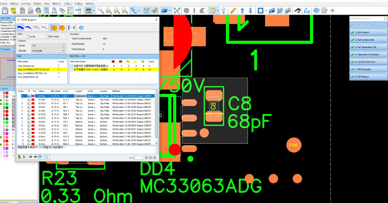
- Use Design Software with DFM Checks: Leverage PCB design tools that include built-in DFM analysis to automatically flag spacing violations or placement issues before fabrication. These tools can catch errors early, saving hours of manual review.
- Collaborate with Manufacturers: Share your design files with your manufacturing partner during the planning stage. Their feedback on component placement can help identify potential issues specific to their equipment or processes.
- Prioritize High-Risk Components: Start placement with critical components like connectors, high-power ICs, or sensitive analog parts. Position them first to ensure optimal spacing and thermal management, then fill in smaller components around them.
- Test with Prototypes: Before full-scale production, create a prototype to validate your placement strategy. Use automated optical inspection (AOI) to check for soldering defects or alignment issues that might not be visible in simulations.
By incorporating these practices into your workflow, you’ll create PCB designs that are not only easier to manufacture but also more reliable and cost-effective.
Common Mistakes to Avoid in Component Placement
Even with the best intentions, it’s easy to overlook certain aspects of component placement. Here are some common mistakes to watch out for when applying PCB manufacturability guidelines.
- Ignoring Manufacturer Specifications: Every manufacturing setup has unique capabilities and limitations. Failing to account for these can lead to placement errors that are only discovered during assembly.
- Overcrowding the Board: Trying to fit too many components into a small space often violates component spacing rules, leading to soldering defects and assembly challenges.
- Neglecting Thermal Management: Placing heat-generating components too close together without proper spacing or heat sinks can cause overheating, reducing the board’s lifespan by up to 50% in extreme cases.
- Inconsistent Orientation: Randomly orienting components increases pick and place machine setup time and raises the risk of placement errors during assembly.
Avoiding these pitfalls will help ensure a smoother manufacturing process and a higher-quality end product.
Conclusion: Mastering DFM Component Placement for Better PCBs
Component placement is more than just arranging parts on a board—it’s a critical factor in achieving efficient, cost-effective, and reliable PCB manufacturing. By adhering to DFM component placement principles, such as following component spacing rules, optimizing for pick and place machines, and ensuring solderability, you can significantly enhance the manufacturability of your designs. These practices not only streamline production but also improve product quality and reduce costs, giving you a competitive edge in any industry.
Start applying these PCB manufacturability guidelines in your next project to see the difference. With careful planning and attention to detail, you can create designs that are easier to build and perform better in the field. At ALLPCB, we’re committed to supporting your journey with resources and expertise to bring your PCB designs to life with precision and efficiency.


