 ALLPCB


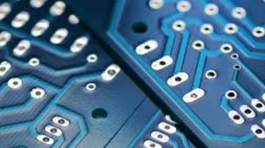
In the fast-evolving world of electronics, creating compact and powerful devices means working with high-density printed circuit boards (PCBs). These boards pack more components into smaller spaces, making soldering a critical and challenging process. So, how do manufacturers achieve precision in such complex designs? The answer lies in selective soldering for high-density PCBs—a technique that targets specific areas for soldering while protecting sensitive components. In this blog, we’ll dive deep into the world of selective soldering, explore its role in advanced PCB assembly, and uncover the techniques and challenges of working with fine pitch and mixed technology boards.
What Is Selective Soldering and Why Does It Matter for High-Density PCBs?
Selective soldering is a specialized process used in PCB assembly to apply solder only to specific areas of a board. Unlike wave soldering, which applies solder across an entire board, or reflow soldering, which is primarily for surface-mount technology (SMT), selective soldering offers pinpoint accuracy. This makes it ideal for high-density PCBs where components are closely packed, and thermal sensitivity is a concern.
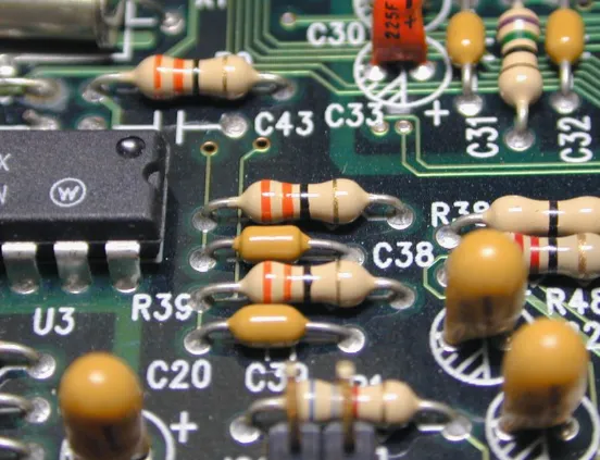
High-density PCBs often feature a mix of SMT and through-hole components, along with fine pitch layouts where the spacing between leads or pads can be as tight as 0.5 mm or less. Traditional soldering methods risk damaging nearby components or creating defects like solder bridges. Selective soldering addresses these issues by using programmable nozzles to deliver molten solder precisely where it’s needed, ensuring reliability and quality in advanced designs.
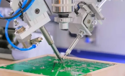
The Basics of Selective Soldering: How It Works
Selective soldering systems typically use a combination of advanced machinery and software to achieve precision. The process involves several key steps:
- Flux Application: A precise amount of flux is applied to the target areas to clean the surfaces and promote solder adhesion.
- Preheating: The board is preheated to reduce thermal shock and ensure even solder flow, often to temperatures around 100-120°C, depending on the materials.
- Soldering: A miniature wave or pinpoint nozzle delivers molten solder (typically at 260-300°C) to specific joints, avoiding sensitive areas.
- Cooling: The board cools down to solidify the solder joints, maintaining structural integrity.
This process is highly automated, with machines using cameras and sensors to align the nozzles with accuracies down to 0.1 mm. This level of control is essential for high-density PCBs, where even a slight misalignment can lead to costly defects.
Selective Soldering vs. Other Techniques: SMT and Through-Hole Soldering
To understand the unique value of selective soldering, it’s helpful to compare it with other common methods like SMT reflow soldering and through-hole wave soldering.
- SMT Reflow Soldering: This technique is widely used for surface-mount components. Solder paste is applied to pads, components are placed, and the board is heated in a reflow oven to melt the solder. While effective for SMT, it’s not suitable for through-hole components or mixed-technology boards often found in high-density designs.
- Through-Hole Wave Soldering: In this method, a PCB passes over a wave of molten solder, which adheres to through-hole component leads. It’s fast and cost-effective for large-scale production but lacks precision and can damage heat-sensitive SMT components on high-density boards.
- Selective Soldering: Combining the benefits of both, selective soldering handles mixed-technology boards by targeting specific through-hole or SMT joints without affecting nearby areas. It’s slower than wave soldering but offers unmatched accuracy for complex assemblies.
For high-density PCBs, where fine pitch components (with lead spacing as low as 0.4 mm) and mixed technologies are common, selective soldering often becomes the go-to choice. It minimizes thermal stress and reduces the risk of defects, ensuring the board performs reliably in demanding applications like telecommunications or medical devices.
The Role of Fine Pitch Soldering in High-Density Designs
Fine pitch soldering refers to the process of soldering components with very close lead or pad spacing, often below 0.65 mm. As devices shrink and performance demands grow, fine pitch components like quad flat no-lead (QFN) packages or ball grid arrays (BGAs) are increasingly common on high-density PCBs. Selective soldering plays a critical role here by delivering solder with extreme precision, avoiding bridges or shorts between adjacent pins.
One key challenge in fine pitch soldering is maintaining consistent solder volume. Too much solder can cause bridging, while too little can result in weak joints. Modern selective soldering systems address this by using adjustable nozzles and real-time monitoring to control solder flow within tolerances of ±0.05 mm. Additionally, the use of nitrogen atmospheres during soldering can reduce oxidation, improving joint quality for fine pitch applications.
PCB Assembly Challenges with High-Density Designs
Assembling high-density PCBs comes with a unique set of challenges, many of which selective soldering is designed to overcome. Let’s explore some of the most common obstacles and how advanced soldering techniques address them.
1. Thermal Management
High-density PCBs generate significant heat due to closely packed components. During soldering, uneven heat distribution can cause thermal shock, warping the board or damaging sensitive parts. Selective soldering mitigates this by preheating the board evenly and applying solder only where needed, keeping temperatures in adjacent areas as low as possible—often below 150°C for sensitive zones.
2. Component Proximity
With components spaced just fractions of a millimeter apart, there’s little room for error. A misplaced solder droplet can create a short circuit, leading to board failure. Selective soldering systems use high-precision nozzles and automated alignment to target joints accurately, reducing the risk of defects even in layouts with densities exceeding 100 components per square inch.
3. Mixed Technology Integration
Many high-density PCBs combine SMT and through-hole components, each requiring different soldering approaches. Selective soldering shines here by handling both types without the need for multiple processes, saving time and reducing handling errors. For instance, it can solder through-hole connectors at 280°C while avoiding nearby SMT chips rated for lower temperatures.
4. Defect Prevention
Defects like solder bridges, insufficient wetting, or cold joints are more likely in high-density designs due to tight tolerances. Selective soldering reduces these risks through programmable parameters, ensuring consistent flux application and solder volume. Studies suggest that selective soldering can lower defect rates by up to 30% compared to manual or wave soldering in complex assemblies.
Advanced Soldering Techniques for High-Density PCBs
Beyond the basics, several advanced soldering techniques enhance the effectiveness of selective soldering for high-density PCBs. These methods push the boundaries of precision and reliability, addressing the needs of cutting-edge electronics.
1. Laser-Assisted Selective Soldering
Laser technology can be integrated with selective soldering systems to heat specific joints without affecting surrounding areas. This is especially useful for fine pitch components, where traditional nozzles might struggle with access. Laser soldering can achieve spot sizes as small as 0.2 mm, ensuring pinpoint accuracy and minimal thermal impact.
2. Multi-Nozzle Configurations
For high-volume production, selective soldering machines with multiple nozzles can target several joints simultaneously. This speeds up the process while maintaining precision, making it viable for medium-scale runs of high-density PCBs. Some systems can handle up to 4 nozzles, each programmable for different solder volumes and temperatures.
3. Real-Time Process Monitoring
Modern selective soldering equipment often includes cameras and sensors for real-time monitoring. These systems detect issues like misalignment or insufficient solder flow during the process, allowing immediate adjustments. This technology can improve first-pass yield rates to over 98%, a critical factor in high-density PCB manufacturing.
4. Nitrogen Shielding
Using a nitrogen environment during soldering reduces oxidation on fine pitch joints, improving solder wetting and joint strength. This technique is particularly beneficial for high-density boards used in harsh environments, such as automotive or aerospace applications, where reliability is non-negotiable.
Benefits of Selective Soldering for High-Density PCB Assembly
Selective soldering offers several advantages that make it a cornerstone of modern PCB assembly, especially for high-density designs:
- Precision: Targets specific joints with accuracies down to 0.1 mm, reducing defects in fine pitch layouts.
- Flexibility: Handles mixed SMT and through-hole components on the same board without multiple setups.
- Reduced Thermal Stress: Minimizes heat exposure to sensitive areas, protecting components with low thermal tolerances.
- Cost-Effectiveness: While slower than wave soldering, it reduces rework and defect costs, saving money in the long run.
- Improved Reliability: Consistent solder joints enhance the performance and lifespan of high-density PCBs in critical applications.
Conclusion: Mastering Precision with Selective Soldering
In the intricate world of high-density PCB assembly, selective soldering stands out as a vital technique for achieving precision and reliability. By targeting specific joints with pinpoint accuracy, it overcomes the challenges of fine pitch soldering, thermal management, and mixed-technology integration. Whether it’s through advanced tools like laser assistance or real-time monitoring, selective soldering continues to evolve, meeting the demands of ever-shrinking, high-performance electronics.
At ALLPCB, we understand the importance of precision in every step of PCB manufacturing and assembly. Our state-of-the-art selective soldering processes ensure that even the most complex high-density designs meet the highest standards of quality. As the electronics industry pushes boundaries, mastering the art of selective soldering remains key to building the future—one precise joint at a time.


