 ALLPCB


If you're tackling a rigid-flex PCB project and facing hurdles like tricky routing, component placement issues, thermal management woes, or EMI interference, you're in the right place. This blog post offers a practical guide to overcoming rigid-flex PCB design challenges with actionable solutions. From optimizing trace routing to shielding against EMI, we’ll dive deep into each aspect to help you achieve a reliable and high-performing design.
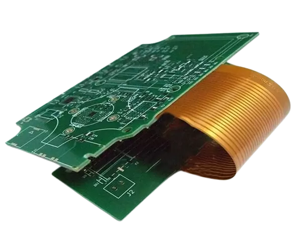
Rigid-flex PCBs combine the best of rigid and flexible circuit boards, enabling compact, durable designs for modern electronics like wearables, medical devices, and aerospace systems. However, their unique structure introduces complexities that can trip up even experienced engineers. Below, we’ll break down the core challenges—routing, component placement, thermal management, and EMI shielding—and provide clear, practical strategies to conquer them.
What Makes Rigid-Flex PCB Design So Challenging?
Rigid-flex PCBs are a hybrid technology, blending rigid sections for structural support and flexible sections for dynamic bending. This combination is ideal for space-constrained applications but creates unique design obstacles. The transition zones between rigid and flex areas are prone to stress, signal integrity issues can arise from varying material properties, and thermal dissipation is often uneven. Add to that the need for precise component placement and protection against electromagnetic interference (EMI), and you've got a design puzzle that demands careful planning.
In this guide, we'll address these pain points head-on with tips and techniques tailored for engineers working on complex assemblies. Whether you're new to rigid-flex or refining an existing design, these insights will help you navigate the process with confidence.
Challenge 1: Routing in Rigid-Flex PCBs
One of the biggest rigid-flex PCB design challenges is routing rigid-flex traces effectively. Unlike traditional rigid boards, rigid-flex designs must account for bending in the flex areas, which can strain traces and lead to cracks or signal loss. Additionally, the transition between rigid and flex sections often causes impedance mismatches, especially in high-speed designs.
Practical Solutions for Routing Rigid-Flex
- Maintain Bend Radius Guidelines: Ensure the flex area’s bend radius is at least 10 times the thickness of the flexible material. For example, with a 0.1 mm thick flex layer, aim for a minimum bend radius of 1 mm to avoid mechanical stress on traces.
- Use Curved Traces in Flex Areas: Straight traces are more likely to crack under repeated bending. Route traces in gentle curves or teardrop shapes at vias to distribute stress evenly.
- Control Impedance: High-speed signals (e.g., operating at 1 GHz or above) require consistent impedance, often around 50 ohms for single-ended signals. Use wider traces or adjust dielectric thickness in flex areas to match impedance with rigid sections.
- Avoid Vias in Bend Zones: Placing vias in flex areas increases the risk of failure. Keep vias in rigid sections whenever possible.
By following these routing strategies, you can minimize signal degradation and mechanical failures, ensuring long-term reliability in your rigid-flex assembly.

Challenge 2: Component Placement in Rigid-Flex Designs
Component placement in rigid-flex designs is another hurdle that can make or break a project. Placing components in the wrong areas can lead to mechanical stress, assembly issues, or inefficient use of space. Since rigid-flex boards are often used in compact devices, every millimeter counts.
Practical Solutions for Component Placement
- Restrict Components to Rigid Areas: Heavy or large components should be placed on rigid sections to avoid stress on the flex material. For instance, connectors or ICs with high pin counts are best suited for rigid zones.
- Optimize for Assembly: Ensure components are spaced to allow for automated pick-and-place machines, typically maintaining at least 0.5 mm clearance between parts for assembly precision.
- Balance Weight Distribution: Uneven weight can cause flex areas to deform over time. Distribute heavier components evenly across rigid sections to maintain structural integrity.
- Consider Flex Orientation: If the flex section will fold during assembly, plan component placement to avoid interference or strain after bending.
Thoughtful component placement not only improves functionality but also simplifies manufacturing, reducing costs and potential errors during production.

Challenge 3: Thermal Management in Rigid-Flex PCBs
Thermal management in rigid-flex designs is critical, especially in high-power applications where heat dissipation varies between rigid and flex materials. Flexible substrates often have lower thermal conductivity (around 0.2 W/m·K compared to 1.5 W/m·K for typical FR-4 rigid material), making it harder to dissipate heat in flex areas.
Practical Solutions for Thermal Management
- Use Thermal Vias in Rigid Areas: Place thermal vias under heat-generating components like power ICs to transfer heat to a ground plane or heat sink. For example, a grid of vias with a 0.3 mm diameter spaced 1 mm apart can significantly improve heat flow.
- Incorporate Copper Planes: Add copper pour areas in rigid sections to act as heat spreaders. A 2 oz copper layer can handle higher thermal loads compared to standard 1 oz copper.
- Select Heat-Resistant Materials: For high-temperature applications, choose flex materials like polyimide, which can withstand temperatures up to 260°C, compared to standard polyester materials that degrade above 150°C.
- Design for Airflow: If the PCB will be enclosed, position heat-sensitive components near ventilation or cutouts in the rigid areas to promote natural convection.
Effective thermal management ensures your rigid-flex PCB operates reliably, even under demanding conditions, extending the lifespan of components and the overall system.
Challenge 4: EMI Shielding in Rigid-Flex PCBs
EMI shielding in rigid-flex designs is a growing concern as devices become more compact and operate at higher frequencies. Electromagnetic interference can disrupt signal integrity, especially in flex areas where grounding is harder to implement. Without proper shielding, sensitive circuits may pick up noise, leading to performance issues.
Practical Solutions for EMI Shielding
- Use Shielding Layers: Incorporate dedicated copper layers or shielding films in the stack-up to block EMI. For instance, a thin 0.025 mm copper layer can reduce interference by up to 30 dB at 1 GHz.
- Ground Planes in Flex Areas: Use cross-hatched ground planes in flex sections to provide a return path for signals while maintaining flexibility. This reduces EMI without compromising the board’s ability to bend.
- Shield High-Speed Traces: Route high-speed signals between ground planes or near grounded copper pours to minimize radiated emissions. Maintain a trace-to-ground spacing of at least 0.2 mm for signals above 500 MHz.
- Apply Conductive Coatings: For additional protection, consider silver ink or conductive polymer coatings on flex areas to create a Faraday cage effect, blocking external interference.
Implementing these EMI shielding techniques helps ensure your rigid-flex PCB performs flawlessly, even in noisy environments like industrial or automotive applications.
Additional Tips for Successful Rigid-Flex PCB Assembly
Beyond addressing specific challenges, a few overarching strategies can streamline your rigid-flex PCB design process and improve outcomes.
- Collaborate Early with Manufacturers: Engage with your PCB fabrication team during the design phase to confirm material availability, stack-up feasibility, and assembly constraints. This can prevent costly redesigns.
- Simulate Before Production: Use simulation tools to model signal integrity, thermal performance, and mechanical stress. For example, simulate a 100 MHz signal to identify potential crosstalk issues before prototyping.
- Test Iteratively: Build and test prototypes under real-world conditions, including bending cycles (e.g., 10,000 cycles for wearables) and temperature extremes (e.g., -40°C to 85°C), to validate your design.
These steps create a robust foundation for tackling even the most complex rigid-flex projects, saving time and resources in the long run.
Conclusion: Mastering Rigid-Flex PCB Design Challenges
Designing and assembling rigid-flex PCBs comes with unique obstacles, from routing rigid-flex traces to managing component placement in rigid-flex, ensuring effective thermal management in rigid-flex, and implementing EMI shielding in rigid-flex. However, with the practical approaches outlined above, you can overcome these rigid-flex PCB design challenges and create reliable, high-performance boards for any application.
Start by prioritizing careful routing with proper bend radii and impedance control. Place components strategically on rigid sections to avoid stress. Address thermal issues with vias, copper planes, and heat-resistant materials. Finally, protect against EMI with shielding layers and grounded designs. By following these guidelines, you’ll be well-equipped to handle the complexities of rigid-flex PCB assembly and deliver innovative solutions for modern electronics.
With the right planning and execution, rigid-flex technology opens up endless possibilities for compact, durable, and efficient designs. Take these strategies into your next project and see the difference they make in performance and reliability.


