 ALLPCB


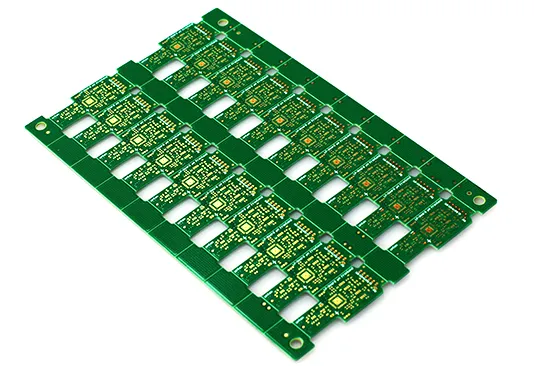
When it comes to manufacturing printed circuit boards (PCBs), one critical step is separating individual boards from a larger panel after production. This process, often called PCB depaneling or PCB panel singulation, ensures that each board is ready for assembly or final use. Two of the most common PCB panel separation methods are V-scoring and tab routing. But which one is the right choice for your project? In short, V-scoring is ideal for simpler, straight-line separations with minimal stress, while tab routing offers flexibility for complex shapes and delicate components, though it may require more finishing work.
In this detailed guide, we’ll dive deep into the differences between V-scoring vs. tab routing PCB methods, explore other PCB depaneling methods, and help you understand the best PCB panel breakout techniques for your needs. Whether you’re an engineer, designer, or manufacturer, this blog will provide actionable insights to optimize your production process.
What Is PCB Panel Separation and Why Does It Matter?
PCB panel separation, also known as depaneling or singulation, is the process of breaking apart individual PCBs from a larger panel used during manufacturing. Panels are created to improve efficiency in production by allowing multiple boards to be processed at once. However, once fabrication and assembly are complete, these boards must be separated without damaging components or the board itself.
Choosing the right PCB panel separation method is crucial because it impacts:
- Board Integrity: Incorrect methods can cause mechanical stress, leading to cracks or damaged traces.
- Production Speed: Some methods are faster and more suited to high-volume runs.
- Cost: Certain techniques require specialized tools or additional finishing steps, affecting overall expenses.
- Component Safety: Delicate or densely populated boards need gentler separation to avoid harm.
With these factors in mind, let’s explore the two primary methods: V-scoring and tab routing.
Understanding V-Scoring: A Simple and Cost-Effective Method
V-scoring is a widely used PCB panel separation method where shallow grooves are cut into both sides of the PCB panel along the separation lines. These grooves, shaped like a “V,” weaken the board at specific points, making it easy to snap the individual boards apart by hand or with a simple tool.
How V-Scoring Works
During manufacturing, a specialized cutting tool creates V-shaped grooves, typically at a depth of about one-third of the board thickness on each side. For a standard 1.6mm thick PCB, this means a groove depth of around 0.5mm per side. The remaining material in the center holds the panel together during production but allows for easy separation later.
Advantages of V-Scoring
- Cost-Effective: V-scoring is inexpensive as it requires minimal tooling and no additional processing after manufacturing.
- Fast Separation: Boards can often be separated manually or with basic equipment, speeding up the process.
- Minimal Stress: When done correctly, V-scoring creates clean breaks with low mechanical stress on components, ideal for boards with standard layouts.
- High-Volume Friendly: It’s well-suited for mass production of rectangular or square boards.
Limitations of V-Scoring
- Limited to Straight Lines: V-scoring only works for straight separation lines, so it’s not suitable for irregular or curved board shapes.
- Risk of Rough Edges: The snapping process can leave slightly rough edges, which may require sanding for aesthetic or functional purposes.
- Not Ideal for Fragile Boards: Boards with delicate components near the scoring line may experience stress during separation.
Best Use Cases for V-Scoring
V-scoring is perfect for simple, rectangular PCB designs in high-volume production where cost and speed are priorities. It’s commonly used in consumer electronics with standard board shapes and layouts.
Exploring Tab Routing: Flexibility for Complex Designs
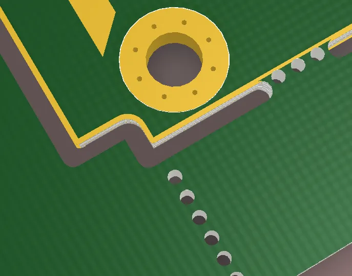
Tab routing, also known as mouse-bite routing, is another popular PCB panel breakout technique. Instead of scoring the entire separation line, small tabs or bridges are left between individual boards in the panel. These tabs hold the boards together during production and are later broken or cut to separate the boards.
How Tab Routing Works
In tab routing, a CNC router cuts out most of the material along the separation line, leaving small connecting tabs (often 2-5mm wide) at intervals. These tabs often include pre-drilled holes, called “mouse bites,” to make breaking easier and reduce stress. After production, the tabs are snapped or cut using pliers or specialized tools.
Advantages of Tab Routing
- Supports Complex Shapes: Unlike V-scoring, tab routing can accommodate irregular or curved board outlines, offering design flexibility.
- Reduced Stress: The small tabs minimize the force needed to separate boards, making it gentler on delicate components compared to snapping a full V-scored line.
- Customizable: Designers can place tabs strategically to avoid sensitive areas of the board.
Limitations of Tab Routing
- Higher Cost: Tab routing requires precise CNC machining, which can increase manufacturing costs compared to V-scoring.
- Additional Finishing: After separation, small tab remnants or burrs often remain on the board edges, requiring manual sanding or filing for a clean finish.
- Slower Process: Both the routing and post-separation cleanup can slow down production, especially for high-volume runs.
Best Use Cases for Tab Routing
Tab routing shines in projects with non-standard board shapes or when components are placed close to the board edges. It’s ideal for prototypes, small-batch production, or designs requiring high precision and minimal stress during separation.
V-Scoring vs. Tab Routing: A Side-by-Side Comparison
To help you decide between these two PCB depaneling methods, let’s compare them across key factors:
| Factor | V-Scoring | Tab Routing |
|---|---|---|
| Cost | Lower cost due to simpler process | Higher cost due to CNC routing |
| Speed | Faster separation, often manual | Slower due to routing and cleanup |
| Design Flexibility | Limited to straight lines | Supports complex shapes |
| Stress on Components | Moderate stress during snapping | Lower stress with proper tab design |
| Edge Finish | May have rough edges | Requires cleanup of tab remnants |
| Best For | High-volume, simple designs | Complex designs, delicate boards |
Other PCB Depaneling Methods to Consider
While V-scoring and tab routing are the most common PCB panel separation methods, other techniques may suit specific needs. Here’s a quick overview:
1. Laser Cutting
Laser cutting uses a focused beam to precisely cut through the PCB material. It’s ideal for ultra-precise separations and complex shapes, with minimal mechanical stress. However, it’s expensive and slower, making it better for low-volume or high-value projects.
2. Punching or Die Cutting
This method uses a custom die to punch out individual boards from the panel. It’s fast for high-volume production but requires costly tooling and setup, and it can cause significant stress on the board.
3. Manual Breaking with Breakaway Rails
Some panels include perforated breakaway rails along the edges, which can be snapped off by hand. This is a low-cost option but offers little precision and can damage components if not designed carefully.
Understanding these alternative PCB panel breakout techniques can help you explore all options before deciding on a method.
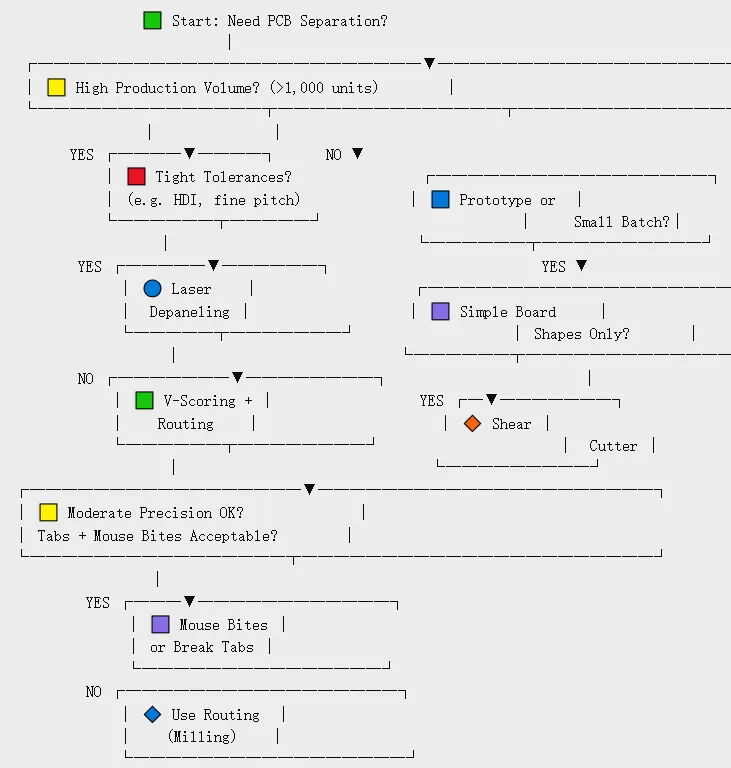
Factors to Consider When Choosing a PCB Panel Separation Method
Selecting the right PCB depaneling method depends on several project-specific factors. Keep these in mind during the design and planning stages:
- Board Design and Shape: If your PCB has an irregular outline, tab routing or laser cutting may be necessary. For straight-edged boards, V-scoring often suffices.
- Component Placement: Components near the board edge are at higher risk of damage during separation. Choose a method like tab routing to minimize stress in these areas.
- Production Volume: High-volume runs benefit from cost-effective methods like V-scoring or punching, while low-volume or prototype runs can justify the cost of tab routing or laser cutting.
- Budget: Balance the cost of the separation method with the overall project budget. Cheaper methods may save money upfront but could lead to higher defect rates if not suited to the design.
- Edge Finish Requirements: If smooth edges are critical for your application, consider the post-separation finishing work each method requires.
Tips for Optimizing PCB Panel Singulation
Regardless of the method you choose, proper planning can improve the depaneling process and reduce risks. Here are some practical tips:
- Design with Separation in Mind: Place components away from separation lines to avoid stress during depaneling. For V-scoring, maintain at least 5mm clearance between components and the score line.
- Test Prototypes: Before full production, test your chosen method on a small batch to identify potential issues like cracking or component damage.
- Specify Tolerances: Work with your manufacturer to define precise tolerances for scoring depth or tab placement. For example, V-scoring depth should not exceed 40% of board thickness per side to prevent premature breaking.
- Use Fiducials: Add fiducial marks on the panel to ensure accurate alignment during routing or scoring, reducing errors in the separation process.
- Plan for Finishing: If edge quality matters, allocate time and resources for sanding or deburring after separation, especially with tab routing.
Conclusion: Making the Right Choice for Your PCB Project
Choosing between V-scoring vs. tab routing PCB separation methods—or any other PCB depaneling methods—comes down to understanding your project’s unique needs. V-scoring offers a cost-effective, fast solution for simple designs and high-volume production, while tab routing provides the flexibility and gentleness required for complex shapes and delicate boards. By considering factors like board design, production volume, and budget, you can select the best PCB panel breakout technique to ensure quality and efficiency.
At ALLPCB, we’re committed to supporting your PCB manufacturing journey with expert guidance and high-quality services. Whether you’re navigating PCB panel singulation or other aspects of production, our team is here to help you achieve the best results. Plan your depaneling strategy early, test your approach, and partner with a trusted manufacturer to bring your designs to life.


