ALLPCB


< there! If you're dealing with via-in-pad issues in your PCB designs, you're in the right place. This guide will help you troubleshoot common problems like solder wicking, solder voids, reliability concerns, and manufacturing defects. Let's dive into practical solutions to get your designs back on track.
Via-in-pad technology is a game-changer in PCB design, especially for high-density layouts where space is tight. By placing vias directly under component pads, you can save board real estate and improve signal integrity. However, this approach comes with challenges like via-in-pad solder wicking, via-in-pad solder voids, via-in-pad reliability issues, and via-in-pad manufacturing defects. In this comprehensive guide, we'll walk you through identifying these problems, understanding their causes, and applying practical solutions to ensure your PCB performs at its best.
What is Via-in-Pad Technology?
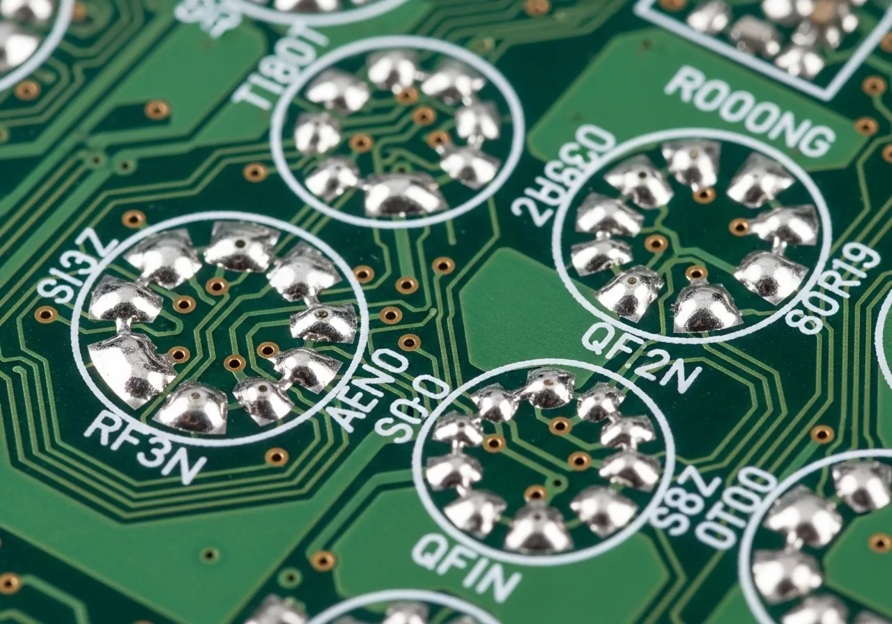
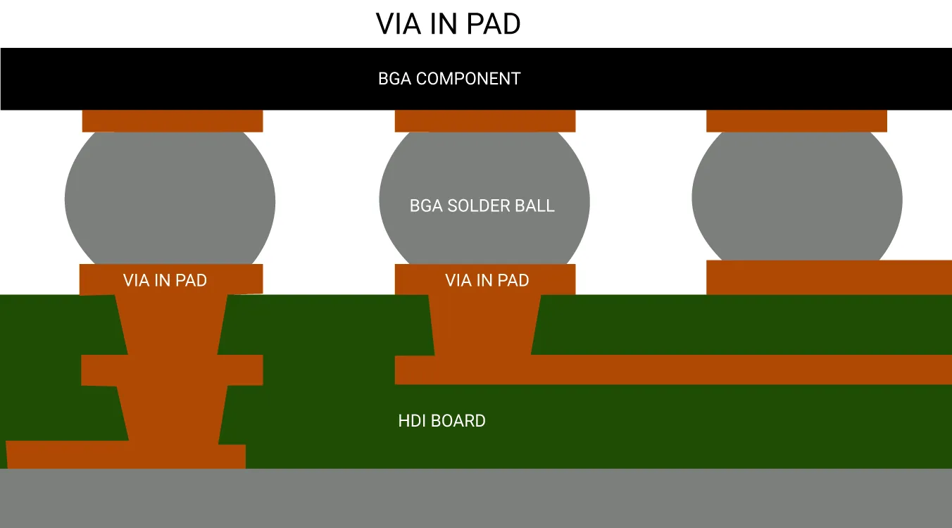
Via-in-pad refers to a PCB design technique where a via—a small hole that connects different layers of a board—is placed directly within the pad of a surface-mount component. This method is often used in high-density interconnect (HDI) designs to reduce the space needed for routing and to shorten signal paths. It's especially common in designs with fine-pitch components like BGAs (Ball Grid Arrays), where traditional via placement outside the pad would consume too much space.
While this technology offers benefits like reduced inductance (often below 0.5 nH compared to 1-2 nH for standard vias) and better thermal management, it introduces unique challenges during manufacturing and assembly. Let’s explore the most common issues and how to troubleshoot them.
Common Via-in-Pad Issues and Their Causes
Before diving into solutions, it's crucial to understand the problems that can arise with via-in-pad designs. Below are the four most frequent issues engineers face.
1. Via-in-Pad Solder Wicking
via-in-pad solder wicking occurs when molten solder flows into the via during the reflow soldering process, leaving insufficient solder on the pad to form a strong joint. This can result in weak or incomplete connections, leading to electrical failures.
Causes:
- Unfilled or improperly filled vias allow solder to escape through the hole.
- Excessive via diameter (e.g., larger than 0.3 mm for a 0.5 mm pad) increases the risk of solder flow.
- Inadequate stencil design or paste volume fails to account for solder loss into the via.
2. Via-in-Pad Solder Voids
via-in-pad solder voids are air pockets or gaps in the solder joint, often caused by outgassing from the via during reflow. These voids can weaken the joint and affect thermal and electrical performance.
Causes:
- Moisture trapped in the via or surrounding materials vaporizes during heating, creating bubbles.
- Poor via filling or plugging leaves space for air to get trapped.
- Inconsistent reflow profiles (e.g., peak temperatures below 240°C for lead-free solder) prevent proper solder flow.
3. Via-in-Pad Reliability Issues
via-in-pad reliability issues refer to long-term performance problems, such as cracks in solder joints or delamination of the via structure, which can lead to failures under thermal or mechanical stress.
Causes:
- Thermal expansion mismatch between materials (e.g., CTE of copper at 17 ppm/°C vs. PCB substrate at 50-70 ppm/°C) causes stress during temperature cycling.
- Weak solder joints from wicking or voids fail under vibration or shock.
- Poor via plating or filling leads to internal defects that worsen over time.
4. Via-in-Pad Manufacturing Defects
via-in-pad manufacturing defects include issues like incomplete via filling, exposed copper, or misalignment, which can compromise the integrity of the PCB during assembly or operation.
Causes:
- Inconsistent via plugging processes, such as using low-quality resin or solder mask, result in voids or cracks.
- Drilling inaccuracies (e.g., tolerances exceeding ±0.05 mm) lead to misaligned vias.
- Insufficient copper plating thickness (below 25 μm) in the via barrel causes weak connections.
Troubleshooting Via-in-Pad Issues: Practical Solutions
Now that we've identified the common problems, let’s explore actionable steps to address each one. These solutions are designed to help engineers optimize their designs and manufacturing processes for better results.
Solving Via-in-Pad Solder Wicking
To prevent via-in-pad solder wicking, focus on controlling the solder flow during assembly. Here are some strategies:
- Use Filled Vias: Ensure vias are filled with conductive or non-conductive material (like epoxy resin) before soldering. Conductive filling can improve thermal and electrical performance, with resistance often below 10 mΩ per via.
- Cap the Via: After filling, cap the via with a thin layer of copper or solder mask to block solder from entering. This process, often called "via-in-pad plated over," is now an industry standard.
- Optimize Stencil Design: Increase solder paste volume by 10-20% on pads with vias to compensate for potential loss. For a 0.5 mm pad, consider a stencil aperture of 0.55-0.6 mm.
- Reduce Via Size: Keep via diameters small (e.g., 0.2-0.3 mm) to minimize solder flow. Check with your manufacturer for drilling capabilities, as smaller vias require tighter tolerances.
Addressing Via-in-Pad Solder Voids
Minimizing via-in-pad solder voids requires attention to both design and assembly conditions. Try these tips:
- Pre-Bake the PCB: Bake boards at 120°C for 2-4 hours before assembly to remove moisture that could cause outgassing. This is especially critical for boards stored in humid environments (above 60% RH).
- Use Proper Via Filling: Ensure vias are completely filled with resin or conductive paste to eliminate air pockets. Incomplete filling can lead to void percentages as high as 20-30% in solder joints.
- Adjust Reflow Profile: Use a reflow profile with a gradual ramp-up rate (1-3°C per second) and a peak temperature of 240-250°C for lead-free solder to allow gases to escape before the solder solidifies.
- Inspect with X-Ray: After assembly, use 2D or 3D X-ray inspection to check for voids. Industry standards like IPC-A-610 accept voiding up to 25% of the joint area for Class 2 products, but aim for less than 10% for high-reliability applications.
Improving Via-in-Pad Reliability Issues
To tackle via-in-pad reliability issues, focus on design and material choices that withstand stress over time:
- Select Compatible Materials: Choose PCB substrates with a coefficient of thermal expansion (CTE) closer to copper, such as high-Tg FR-4 (CTE around 40-50 ppm/°C), to reduce stress during thermal cycling (-40°C to 85°C typical range).
- Reinforce Solder Joints: Avoid wicking and voids by following the steps above, as strong joints are less likely to crack under vibration (tested at 10-55 Hz per IPC standards).
- Test for Reliability: Conduct thermal cycling tests (e.g., 1000 cycles between -40°C and 125°C) and drop tests to simulate real-world conditions. Monitor for failures using microsection analysis to spot cracks or delamination.
- Use Thicker Plating: Ensure via barrel plating is at least 25 μm thick to prevent cracking under mechanical stress. Thinner plating can lead to open circuits after just a few thermal cycles.
Fixing Via-in-Pad Manufacturing Defects
Preventing via-in-pad manufacturing defects starts with clear communication with your fabrication partner and strict quality control:
- Specify Via Filling Process: Clearly define whether vias should be filled with conductive paste, epoxy, or solder mask in your design files. Include notes on capping if needed to avoid exposed copper, which can lead to shorts.
- Set Tight Tolerances: Work with your manufacturer to ensure drilling accuracy within ±0.05 mm. Misaligned vias can shift pads by 0.1 mm or more, causing assembly issues.
- Perform AOI and Testing: Use Automated Optical Inspection (AOI) during fabrication to catch defects like incomplete filling or exposed copper. Follow up with electrical testing to confirm via continuity (resistance below 10 mΩ).
- Review DFM Guidelines: Follow Design for Manufacturability (DFM) rules, such as maintaining a minimum annular ring of 0.1 mm around vias, to ensure proper pad integrity during drilling and plating.
Best Practices for Via-in-Pad Design
Beyond troubleshooting specific issues, adopting these best practices in your initial design phase can prevent problems from arising:
- Limit Via-in-Pad Use: Only use this technique when necessary, such as for fine-pitch components (below 0.5 mm pitch) or HDI designs. For larger components, traditional vias outside pads are often more reliable.
- Collaborate Early: Share your design files with your PCB manufacturer during the planning stage to confirm their capabilities for via filling, plating, and tolerances.
- Simulate Signal Integrity: Use simulation tools to verify that via-in-pad placement doesn’t introduce signal reflection or crosstalk, especially for high-speed designs above 1 GHz.
- Document Everything: Include detailed notes in your Gerber files and BOM about via treatment (e.g., "fill and cap all vias under BGA pads") to avoid miscommunication during fabrication.
Conclusion
Via-in-pad technology offers significant advantages for compact, high-performance PCB designs, but it requires careful attention to detail to avoid pitfalls like via-in-pad solder wicking, via-in-pad solder voids, via-in-pad reliability issues, and via-in-pad manufacturing defects. By understanding the root causes of these problems and applying the troubleshooting steps outlined in this guide, you can achieve robust and reliable designs that meet your project goals.
From optimizing solder paste application to ensuring proper via filling and conducting thorough inspections, each step plays a vital role in the success of your PCB. Incorporate these practices into your workflow, and you’ll be well-equipped to handle the challenges of via-in-pad technology. Let’s build better boards together!